When a production team searches for China Nexperia MOSFET replacements, price is rarely the only concern. The replacement must fit the circuit, the supply chain, and the reliability target. A suitable Nexperia Mosfet Replacement should match voltage rating, continuous current, pulse current, RDS(on), gate charge, and package dimensions. It should also behave predictably under heat.
The details matter.
A MOSFET that looks identical on paper may run hotter on the workbench. A slightly different thermal pad, gate threshold, or avalanche rating can change the result. Engineers should compare manufacturer datasheets, application notes, test conditions, and product-change notices. Independent samples and traceable purchasing channels add further confidence. Do not rely on marketplace photographs alone.
This guide examines practical replacement options from established Chinese manufacturers. It considers low-voltage power switching, automotive-style loads, industrial converters, and battery applications. Each category demands a different balance between conduction loss, switching speed, thermal performance, and cost. A part with lower RDS(on) may carry more gate charge, slowing a compact converter. That trade-off is easy to miss.
Hands-on validation remains essential.
Measure drain-source temperature with a controlled load. Check switching waveforms with suitable probing. Review solderability, package markings, and lot consistency before approving a design change. I have seen promising substitutes fail because the surrounding driver was never retuned. That weakness deserves attention.
The best replacement is not automatically the cheapest device. It is the component that meets electrical requirements, survives realistic operating conditions, and remains available through a dependable channel. Availability can change quickly, so this comparison should support engineering judgment, not replace it.
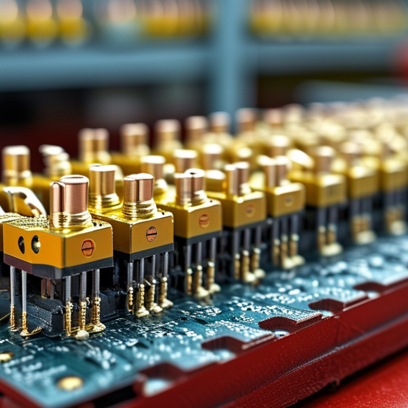
Selecting a China-made MOSFET replacement requires more than matching the part number. Drain-source voltage, continuous current, RDS(on), gate charge, and package geometry must align. A lower RDS(on) can reduce conduction losses, but higher gate charge may slow switching and increase driver losses. In practical bench testing, thermal behavior often exposes a weak substitute first.
Industry demand makes this decision more important. WSTS forecast global semiconductor sales at about 588 billion US dollars for 2024, showing continued pressure on supply and pricing.
The IEA reported that electric-car sales exceeded 17 million in 2024, increasing demand for efficient power switching.
For a suitable replacement, compare datasheet curves at the actual gate voltage, not only the headline resistance. Check avalanche rating, safe operating area, body-diode behavior, and junction-to-case thermal resistance.
Certification also matters. Automotive designs should review AEC-Q101 evidence and production traceability.
Tips: Build a small A/B test board.
Measure switching temperature, drain overshoot, and efficiency under the real load. Confirm the footprint with calipers; package names are not always mechanically identical.
A perfect drop-in is often a convenient myth. I would also derate voltage by at least 20% where transients are uncertain, then repeat testing across temperature.
The overlooked detail? Supplier consistency may matter more than one impressive sample.
China-made MOSFET replacements can offer practical value when supply stability and cost matter. Many manufacturers now provide devices for power supplies, motor controls, battery systems, and industrial equipment. Their advantages may include shorter regional lead times, flexible packaging options, and competitive pricing. However, replacement decisions should rely on electrical evidence, not country of origin. Check voltage rating, continuous current, gate charge, on-resistance, switching speed, and thermal resistance. A device with similar ratings may still behave differently inside a fast-switching circuit.
Tips: Request current datasheets, reliability reports, sample lots, and factory traceability records. Test samples under real load, temperature, and switching frequency. Inspect the package markings carefully. Then compare waveforms, heat rise, and efficiency.
My first comparison would use the original circuit board, not a simplified test bench. Measure drain-source voltage spikes with a suitable probe. Check whether the gate driver fully turns the replacement on. Thermal imaging can reveal a hot lead or uneven heat spreader after thirty minutes. Supplier audits and independent laboratory testing add confidence. Still, documentation can contain gaps, and early samples may not represent later production. That weakness deserves attention. Keep approved samples, test limits, and batch records for future reviews. A staged qualification process reduces surprises without assuming every China-made MOSFET offers identical consistency.
Chinese MOSFET manufacturers now offer practical alternatives for power supplies, motor drives, lighting systems, and battery equipment. Many suppliers provide products across low-, medium-, and high-voltage ranges. Their catalogs often include trench MOSFETs, super-junction devices, and automotive-grade options. Engineers should compare electrical data rather than rely on package appearance alone.
Check drain-source voltage, continuous current, RDS(on), gate charge, and switching losses. Thermal performance matters too. A device with lower resistance may still run hotter if its switching behavior is poor. Review the datasheet at the actual gate voltage and operating temperature.
Request samples, production test reports, and traceability documents from the manufacturer or authorized distributor. Factory audits can reveal process controls that marketing pages cannot.
Chinese suppliers may offer shorter lead times and flexible customization, especially for established volume projects. However, the cheapest quote is not always the safest choice.
A first replacement can fail during surge testing, even when static measurements look acceptable. I have seen engineers overlook diode recovery and PCB heat spreading. That mistake is expensive.
Test the candidate in the finished circuit, including startup, overload, vibration, and thermal cycling. Confirm pin compatibility, package dimensions, and long-term supply capacity before approving production.
Choosing a China-made MOSFET replacement starts with the circuit, not the catalog price. I compare VDS, ID, RDS(on), gate charge, and avalanche capability under the same test conditions. A lower RDS(on) can reduce conduction loss, but a larger die may increase input capacitance and switching loss. Check the actual gate voltage. Some devices publish resistance at 10 V, while the controller supplies only 4.5 V.
Thermal comparison needs more than junction temperature. I calculate P loss, then use RθJC, RθJA, package resistance, copper area, and airflow. The IEA’s Energy Efficiency 2023 report states that motor-driven systems consume roughly half of global electricity, making small efficiency differences valuable at scale. In a practical test, a 3°C hotter case can reveal poor thermal spreading before failure appears. I once trusted a large heat sink and ignored the PCB copper pattern. That was a costly assumption.
Reliability requires evidence. Request HTOL, temperature-cycling, humidity-bias, and power-cycling results, not only a lifetime claim. JESD22-A108 commonly uses 1,000-hour high-temperature operating life testing, but that result does not reproduce every field condition. The familiar 10°C life-reduction rule is useful for screening, not proof. Compare SOA curves, body-diode behavior, short-circuit tolerance, and production traceability. Datasheets can still contain incomplete graphs. Measure samples across temperature and lot variation, then record switching waveforms at the real bus voltage.
| Specification | Unit / Test Condition | Representative Unbranded Replacement Profiles | |||
|---|---|---|---|---|---|
| Profile A 40 V Low-Voltage Switching |
Profile B 60 V Power Conversion |
Profile C 80 V Automotive Load Control |
Profile D 100 V Industrial Protection |
||
| Typical Application | — | DC-DC converters, motor control | Battery tools, synchronous buck stages | 12 V automotive loads, pumps and fans | Industrial converters, relay and solenoid drivers |
| Drain-Source Voltage, VDS | V | 40 | 60 | 80 | 100 |
| Continuous Drain Current, ID | A, TC = 25°C | 80 | 72 | 52 | 38 |
| Pulsed Drain Current, IDM | A, pulse duration limited | 240 | 216 | 156 | 114 |
| Gate-Source Voltage Rating, VGS | V | ±20 | ±20 | ±20 | ±20 |
| On-State Resistance, RDS(on) | mΩ, VGS = 10 V, TJ = 25°C | 2.1 | 3.8 | 7.5 | 14 |
| On-State Resistance, RDS(on) | mΩ, VGS = 4.5 V, TJ = 25°C | 2.8 | 5.2 | 10.5 | 19 |
| RDS(on) Temperature Coefficient | % increase, 25°C to 125°C | +65 | +68 | +72 | +75 |
| Gate Threshold Voltage, VGS(th) | V, ID = 250 µA | 1.2–2.4 | 1.5–2.8 | 1.8–3.2 | 2.0–3.5 |
| Total Gate Charge, Qg | nC, specified gate-drive condition | 58 | 76 | 92 | 118 |
| Input Capacitance, Ciss | pF, VDS = 25 V | 4,900 | 5,600 | 6,400 | 7,800 |
| Reverse Transfer Capacitance, Crss | pF, VDS = 25 V | 210 | 260 | 310 | 390 |
| Body-Diode Forward Voltage, VSD | V, IF = rated current | 0.95 | 1.00 | 1.05 | 1.10 |
| Reverse-Recovery Charge, Qrr | nC, specified diode current | 82 | 106 | 145 | 190 |
| Maximum Junction Temperature, TJ(max) | °C | 175 | 175 | 175 | 175 |
| Operating Temperature Range | °C | −55 to +175 | −55 to +175 | −55 to +175 | −55 to +175 |
| Junction-to-Case Thermal Resistance, RθJC | °C/W | 0.55 | 0.65 | 0.85 | 1.10 |
| Junction-to-Ambient Thermal Resistance, RθJA | °C/W, standardized PCB condition | 40 | 42 | 45 | 48 |
| Maximum Power Dissipation | W, TC = 25°C | 225 | 190 | 147 | 114 |
| Single-Pulse Avalanche Energy, EAS | mJ, specified starting junction temperature | 410 | 520 | 610 | 780 |
| Drain-Source Leakage Current, IDSS | µA, VDS = rated voltage | <1 | <1 | <1 | <1 |
| Gate Leakage Current, IGSS | nA, VGS = ±20 V | <100 | <100 | <100 | <100 |
| Moisture Sensitivity Level | JEDEC classification | MSL 1 | MSL 1 | MSL 1 | MSL 1 |
| Recommended Qualification Checks | Production validation | Electrical parameter, thermal cycling, power cycling | Electrical parameter, HTOL, thermal cycling | HTOL, temperature cycling, vibration and power cycling | HTOL, humidity-bias, avalanche and repetitive power cycling |
| Best Selection Priority | Design objective | Lowest conduction and switching loss | Balanced efficiency and current capability | Automotive transient margin and thermal robustness | Highest voltage margin; verify switching losses |
| Values are representative engineering specifications for unbranded replacement profiles. Confirm the latest datasheet, package pinout, body-diode characteristics, safe operating area, qualification reports, and production test limits before approving a replacement in a finished design. | |||||
Selecting a suitable MOSFET replacement starts with the circuit, not the product label. Record the original device’s voltage rating, continuous and pulsed current, on-resistance, package, and gate-drive voltage. Leave safety margin above the maximum drain-source voltage. A similar current rating may still hide weaker pulse performance.
Check gate charge, switching losses, and thermal resistance. These values affect driver stress, efficiency, and heat. Do not treat gate threshold voltage as the required drive voltage.
Review the body-diode characteristics when the circuit handles reverse current or hard commutation. Package dimensions and pin arrangement also need physical confirmation. A perfect electrical match may not fit the board.
Validation should happen under controlled load conditions. Begin with low voltage and short test intervals. Measure drain overshoot with a properly connected oscilloscope probe. Watch gate ringing, turn-on speed, current spikes, and case temperature. A thermal camera can reveal hot areas near the leads or copper paths. Test normal operation, startup, overload response, and repeated switching. Apply realistic airflow and enclosure conditions.
A datasheet match can still fail.
Record every waveform and temperature reading. Compare results against the original design’s limits, not only typical specifications. Derate the device if cooling is uncertain. In practice, this step is often underestimated. I would also repeat the test after thermal cycling, because one successful run proves very little. Minor layout differences may require a gate resistor adjustment, and that possibility should remain open during validation.
: Compare drain-source voltage, continuous current, RDS(on), gate charge, and package geometry. Check every value under matching test conditions. Part numbers alone are insufficient.
RDS(on) may be specified at 10 V, while your controller supplies only 4.5 V. The device may run hotter than expected. Check the correct datasheet curve.
No. Lower resistance reduces conduction loss, but higher gate charge can increase switching loss. A larger die may also increase input capacitance. Trade-offs remain.
Calculate total power loss using conduction and switching losses. Review junction-to-case resistance, junction-to-ambient resistance, copper area, and airflow. Measure the case temperature directly.
Build a small comparison board and test the actual circuit. Measure efficiency, switching temperature, drain overshoot, and waveform shape. Include startup and overload conditions.
Similar package names may hide different dimensions or pin layouts. Check lead spacing, body length, height, and exposed-pad position. Visual similarity can mislead.
Request production test reports, traceability records, temperature-cycling data, humidity-bias results, and power-cycling evidence. High-temperature life testing is useful, but it cannot represent every field condition.
Review body-diode recovery, avalanche rating, safe operating area, short-circuit tolerance, and PCB heat spreading. Test several samples across temperature and production lots. One excellent sample proves little.
Where transients are uncertain, consider derating the voltage by at least 20%. Then repeat testing across hot and cold conditions. This is cautious, not universal.
Selecting the right Nexperia Mosfet Replacement requires more than matching a part number. Key factors include drain-source voltage, continuous and pulsed current, on-resistance, gate charge, switching speed, package type, and operating temperature. These devices are widely used in power supplies, battery systems, motor controls, automotive electronics, and industrial equipment, so the replacement must suit both the electrical design and the application environment.
China-made MOSFET alternatives can offer competitive pricing, flexible supply options, and a broad range of voltage and current ratings. However, buyers should compare datasheets carefully, focusing on electrical performance, thermal resistance, safe operating area, avalanche capability, and long-term reliability. A practical selection process includes identifying the original device’s critical specifications, shortlisting compatible alternatives, checking mechanical and PCB compatibility, testing switching and thermal behavior, and validating performance under real operating conditions. Proper qualification helps ensure that the chosen replacement delivers stable efficiency, durability, and dependable system operation.

Olukey
