Explore our leading N-Channel and P-Channel integration solutions, optimized for high efficiency, compact thermal design, and robust reliability.
In modern power electronic topologies, the synchronous combination of N-Channel and P-Channel Metal-Oxide-Semiconductor Field-Effect Transistors (MOSFETs) is vital for efficient electrical conversion. N-Channel MOSFETs rely on high-mobility free electrons as major charge carriers, offering lower RDS(on) values and minimal dynamic power dissipation. Conversely, P-Channel MOSFETs operate via hole transport, which naturally exhibits roughly half to one-third the mobility of electrons under equivalent electric field intensities.
Matching the switching dynamics of these complementary pairs is a primary manufacturing challenge. Modern fabrication facilities focus on tailoring gate charge (Qg) and internal gate resistance (Rg) so that P-channel switching times align with N-channel performance, mitigating cross-conduction (shoot-through) issues in driver and synchronous buck architectures.

Understanding how Olukey Industry aligns Winsok MOSFET technologies with macro-industrial trends and global logistics networks.
HONGKONG Olukey INDUSTRY CO., LIMITED is a solution provider focusing on the overall solution of electronic product components. The main products mainly include: WINSOK MOSFET, Cmsemicon MCU, PCBA circuit board solution development and other three types of product lines. Currently, the products of Olukey Industry are widely used in automotive electronics, military electronics, smart industry, new energy, smart medical care, 5G, Internet of Things, smart home, and various consumer electronics products.
Relying on the advantages of global general agents of major original factories, we are based in the Asia-Pacific market. Provide customers with various advanced high-tech electronic components by using comprehensive superior services, assist manufacturers in producing high-quality products and provide comprehensive services.




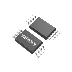
WINSOK MOSFET's product voltages are mainly medium and low voltage: 15V, 20V, 30V, 40V, 60V, 80V, 100V, 120V, 150V, 200V, 250V, 300V, 400V, 500V, 600V, 650V. The main packages include DFN3X3-8, DFN5X6-8, TO-252, TO-263, SOP-8, SOT-23, TO-220, etc. There are more than 600 models and more than 40 packages. Extensive coverage of medium-voltage and low-voltage MOSFET product lines on the market.
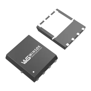
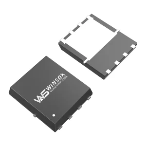
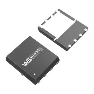
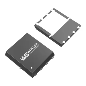
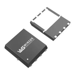
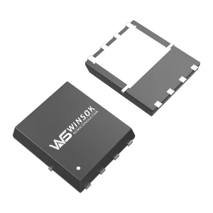
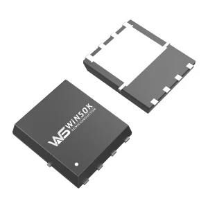
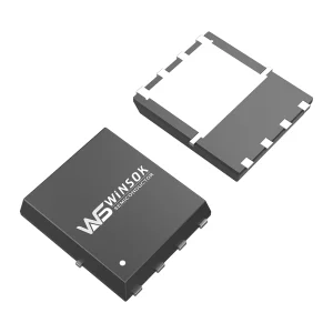
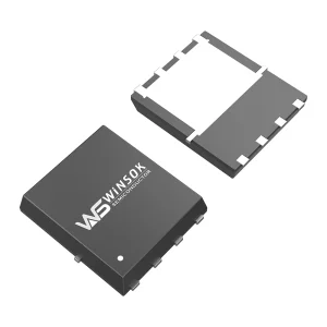
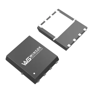
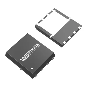
Inside advanced assembly facilities, packing complementary N-Channel and P-Channel silicon dies into tight form factors like the DFN5x6-8 or DFN3x3-8L requires highly precise die attach technology. Copper clip bonding technology has replaced traditional wire bonds, significantly minimizing internal package source-inductance, reducing RDS(on), and allowing symmetric heat dispersion from the dual silicon structure.
Our factories employ automatic optical inspection (AOI) alongside dynamic testing systems to guarantee high reliability under harsh thermal cycles, mitigating risks of early component failure in industrial and automotive projects.
Combining design capabilities, deep component distribution experience, and global chipmaker partnerships.
Relying on the advantages of global general agents of major original manufacturers, we are based on the Asia-Pacific market. Through active market development and effective resource integration, we have become one of the outstanding agents in the region.
Cmsemicon MCU is a microcontroller company born in Shenzhen, with rich product types and technology R&D experience. We assist clients by pairing microcontrollers with our MOSFET arrays for optimum PCBA solution designs.
We use our comprehensive advantageous services to provide customers with various types of advanced high-tech electronic components, assist manufacturers in producing high-quality products and provide comprehensive after-sales technical support.
Where complementary N-Channel and P-Channel MOSFET modules are widely deployed across industries.
In robotics, automotive window regulators, and smart home appliances, H-bridge circuits dictate DC motor direction. Using two P-channels on the high-side and two N-channels on the low-side simplifies driver layout. High-side gate driver bootstrap circuits are eliminated, decreasing BOM costs and streamlining the design.
Power rail management in smart medical systems and 5G telecommunication hardware requires fast, low-loss switching. P-Channel MOSFETs act as ideal high-side switches since they are controlled relative to the source voltage, simplifying control logic directly from microcontrollers (MCU).
To supply clean voltage rails to mobile electronics and advanced processing units, dual N+P channel structures in DFN3x3 or DFN5x6 packages are deployed in DC-DC buck regulators. They optimize conversion efficiency, reduce package footprint, and improve dynamic loop stability.
As a global value agent, Hongkong Olukey Industry Co., Limited prioritizes strict regulatory adherence and localized engineering assistance. Our components conform to strict international directives, including RoHS, REACH, and custom automotive-grade standards where applicable.
We run local technical application labs to help customers analyze EMI anomalies, evaluate thermal limits, and carry out safe switching-crossover checks. Our distribution hubs across key technological regions enable shortened lead times, buffering manufacturers from volatile global logistics disruptions.

The strategic development and structural evolutions of next-generation power MOSFETs.
Addressing engineering designs, factory specifications, and application integration challenges.
Select from our complete range of dual-channel packages, designed to support high current capacity and efficient thermal management.
 Olukey