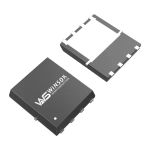
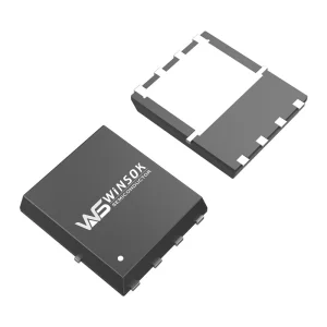
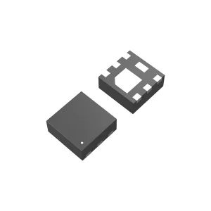
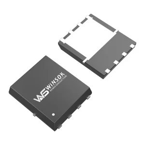
High-efficiency switching transistors in optimized packaging, engineered for thermal performance, low gate charge, and minimal drain-to-source on-resistance.


HONGKONG Olukey INDUSTRY CO., LIMITED is an industry-leading integrated solution provider focusing on the overall layout and design of premium electronic components. With years of fabrication and packaging expertise, our capabilities center around three primary pillars: WINSOK MOSFET, Cmsemicon MCU, and comprehensive PCBA circuit board solutions.
At present, Olukey Industry's advanced solutions are deployed across complex sectors, including automotive electronics, military electronics, smart industrial control systems, new energy conversion systems, smart medical applications, 5G infrastructures, IoT nodes, smart home appliances, and consumer electronics. Operating through strategic alliances with major global agent networks and domestic semiconductor foundries, we serve the entire Asia-Pacific and international markets. Our technical commitment ensures prompt component accessibility, helping manufacturers execute designs with optimal cost-to-performance efficiency.
How modern hardware designers and supply chain executives navigate high-density power requirements and alternate sourcing strategies.
Recent supply disruptions have pushed B2B purchasing managers to look for trusted second-source manufacturers that can provide high pin-to-pin compatibility with major tier-1 brands, avoiding single-point manufacturing failures.
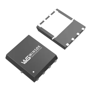
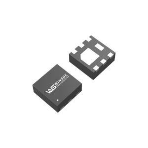
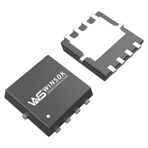
As operating parameters shrink, heat dissipation is critical. Engineers demand low RDS(on) switching nodes and advanced packages (like DFN3X3 and DFN5X6) to minimize parasitics and maximize efficiency.
For automotive electronic components, manufacturers must deliver rigorous qualifications, certified testing procedures, and robust material analysis records to guarantee operation in harsh vehicle environments.
At Olukey Industry, we use comprehensive high-quality services to provide customers with various types of advanced high-tech electronic components, assist manufacturers in producing high-quality products and provide comprehensive services. Over the years, the company has relied on reputation to survive, adhering to the tenet of "quality first, service first", and has established good cooperative relationships with many high-tech enterprises and original manufacturers at home and abroad.
By controlling wafer fabrication, maintaining state-of-the-art packaging lines, and implementing thorough post-packaging stress testing, we reduce failures to parts-per-billion levels. Our logistics and engineering hubs ensure that customers get continuous support, starting from initial prototyping phases all the way through to mass production stages.
Combining WINSOK MOSFETs with Cmsemicon MCU design pathways enables us to offer pre-configured, optimized power stages. This unique combination decreases board area, lowers parasitic inductance, and accelerates overall development timelines.

Leveraging deep relationships with original semiconductor manufacturers and advanced packaging foundries to deliver reliable components.
Relying on the advantages of global general agents of major original manufacturers, we are based on the Asia-Pacific market. Through active market development and effective resource integration, it has become one of the outstanding and fast-growing agents in the Asia-Pacific region. The company has many years of professional distribution experience. We use our comprehensive advantageous services to provide customers with various types of advanced high-tech electronic components, assist manufacturers in producing high-quality products and provide comprehensive services.
WINSOK MOSFET's product voltages are mainly medium and low voltage: 15V, 20V, 30V, 40V, 60V, 80V, 100V, 120V, 150V, 200V, 250V, 300V, 400V, 500V, 600V, 650V. The main packages include DFN3X3-8, DFN5X6-8, TO-252, TO-263, SOP-8, SOT-23, TO-220, etc. There are more than 600 models and more than 40 packages. Extensive coverage of medium-voltage and low-voltage MOSFET product lines on the market.
Cmsemicon MCU is a microcontroller company born in Shenzhen, with rich product types and technology research and development experience. Becoming a global high-value agent is the common goal pursued by OLUKEY Industrial employees. We adhere to the corporate values of "Pragmatism, Win-win, Service and Responsibility", continue to strengthen service quality, and aim to provide high-quality services. Work hand in hand with suppliers to jointly explore a larger market and contribute to the prosperity and development of semiconductors.




Optimizing operating topologies across complex high-voltage switching, automotive drive systems, and power-sensitive IoT nodes.
With vehicles transitioning to electrical architectures, low-loss MOSFETs (15V to 100V) are widely deployed in electric power steering (EPS), motor control stages, LED lighting systems, and DC-DC converters. Advanced packaging supports thermal cycling without weld failures.
In high-power industrial designs, switching losses can significantly impact system performance. Utilizing TO-220 and TO-263 packages with low RDS(on) ensures reliable thermal performance in solar micro-inverters, industrial motor drives, and advanced battery management systems (BMS).
Base stations and network hardware call for highly reliable power supplies. Our high-voltage MOSFET configurations (up to 650V) are key components in power factor correction (PFC) blocks and LLC resonant converters, helping telecom platforms optimize their operating uptime.
A detailed technical comparison of the performance characteristics, parasitic parameters, and applications of key packaging variants.
| Package Type | Voltage Ranges | Typical RDS(on) Range | Thermal Resistance (RthJC) | Primary Target Applications |
|---|---|---|---|---|
| DFN2X2 / DFN3X3 | 15V - 40V | < 8.5 mΩ | 3.2 - 4.5 °C/W | Mobile hand-held units, IoT power nodes, wearable device charging systems. |
| DFN5X6-8L | 30V - 150V | < 1.8 mΩ | 1.1 - 1.8 °C/W | High-density DC-DC buck stages, synchronous rectification, automotive EPS. |
| SOP-8 / SOT-23 | 20V - 60V | < 25 mΩ | 25 - 40 °C/W | LED panel illumination, consumer smart electronics, peripheral power rails. |
| TO-252 (DPAK) | 30V - 250V | < 4.2 mΩ | 1.5 - 2.5 °C/W | Brushless motor control systems, battery management modules, low-power chargers. |
| TO-220 / TO-263 | 100V - 650V | < 0.85 Ω (High V) | < 0.65 °C/W | LLC power topologies, telecom PFC platforms, server power backplanes, inverters. |
How we are engineering the future of silicon designs to enable higher power density, lower switching losses, and robust reliability.
By thinning wafers down to sub-100µm levels, we significantly lower the vertical drift region resistance. This structural upgrade allows next-generation designs to reduce on-resistance while maintaining robust avalanche characteristics.
By reducing gate-to-drain overlap capacitance (Cgd), we minimize the total gate charge (Qg). This allows hardware engineers to design faster switching systems without experiencing excessive transient heating.
While silicon remains essential, our development path integrates hybrid Silicon-Silicon Carbide (SiC) options. This provides power system designers with high-frequency solutions for next-generation green energy architectures.

With distribution channels spanning major regions, we provide reliable logistical support to key manufacturing hubs. Our warehouses are strategically positioned in Hong Kong, Shenzhen, and major industrial centers across the Asia-Pacific region, allowing us to maintain stable lead times and minimize supply disruptions.
Every product batch is trackable, with detailed test certificates, electrical parameter distributions, and environmental compliance documentation (including RoHS and REACH declarations) available. Our engineering teams help you identify pin-to-pin compatible alternatives to simplify development and minimize supply chain risks.
We perform rigorous inspections on incoming wafers, monitor processing parameters in real-time, and run automated testing protocols. This structured quality process ensures consistent electrical parameters and reliable operation in demanding field applications.
Detailed answers to key technical questions from hardware engineers, layout specialists, and supply chain professionals.
Dual-channel configurations integrate two independent N-channel or P-channel transistors into a single package, such as the DFN3x3 or DFN5x6. This layout configuration reduces parasitic trace inductance and minimizes the physical board area by up to 50%, making it an ideal choice for compact power converters, motor drives, and space-constrained smart applications.
Trench-gate architectures construct vertical channel paths directly in the silicon drift region. This design increases channel density per unit area, significantly reducing RDS(on). It also reduces total gate charge (Qg), enabling faster switching speeds and lower power dissipation in high-efficiency power converters.
Gate charge represents the total charge required to fully turn on the transistor channel. Lower gate charge (Qg) reduces transition times between on and off states. This directly decreases switching losses, making it easier to design high-frequency, high-efficiency power stages.
Yes. Our product line is designed to offer high pin-to-pin and thermal compatibility with major industry alternatives. Our engineers can provide cross-reference guides to help you identify replacement options for existing designs, simplifying supply chain management.
We subject our products to standard reliability testing protocols, including High-Temperature Reverse Bias (HTRB), High-Temperature Gate Bias (HTGB), and thermal shock cycling. These tests help ensure that our MOSFETs deliver stable performance over their entire operating lifetime.
Designers should focus on the junction-to-case thermal resistance (RthJC). Using packages with low RthJC values, like the DFN5x6 or TO-220, helps efficiently transfer heat away from the silicon die. This keeps junction temperatures within safe limits, improving overall system reliability.
Browse our additional range of P-channel, N-channel, and dual configurations, available in standard packages for industrial and power electronics applications.
 Olukey