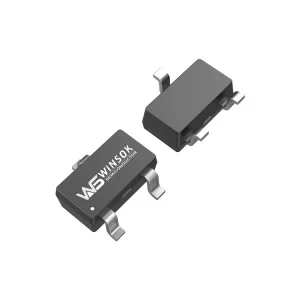
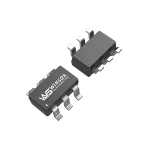
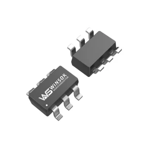
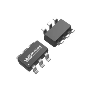
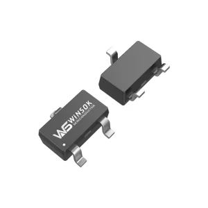
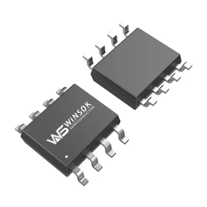
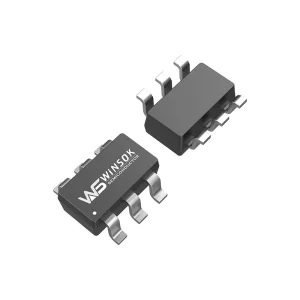
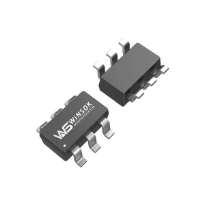
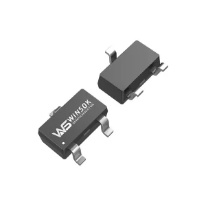
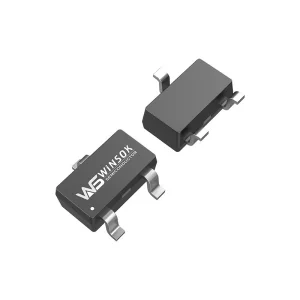
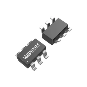
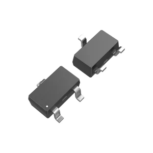
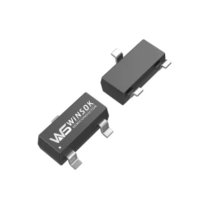
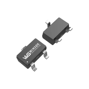
Explore our premium range of SOT-packaged N-channel, P-channel, and complementary dual MOSFETs immediately available for high-throughput procurement.
In modern high-density power electronics design, the selection of discrete semiconductor packaging acts as a primary determinant of system thermal management, efficiency limits, and footprint constraints. Small Outline Transistor (SOT) package MOSFETs, particularly the SOT-23 family (including SOT-23-3L, SOT-23-6L, and SOT-23N), serve as the foundational building blocks for low-to-medium power conversion applications globally.
While newer packaging technologies like DFN (Dual Flat No-leads) have gained traction due to their slightly reduced parasitic inductance, SOT packages remain uniquely dominant for several key reasons:
When selecting SOT package MOSFETs, electrical engineering groups prioritize the minimization of $R_{DS(ON)}$ (drain-source on-resistance) and the optimization of the total gate charge ($Q_g$) to decrease conduction and switching losses, respectively. WINSOK’s structural design utilizes high-cell-density trench technology to achieve class-leading silicon performance values within standard SOT configurations.
| Package Code | Standard Configuration | Common Channel Types | Primary Application Areas | Voltage Envelope |
|---|---|---|---|---|
| SOT-23-3L | Single Die (3 Leads) | N-Channel, P-Channel | Load Switch, Battery Protection, Small Signal Boost | 15V - 100V |
| SOT-23-6L | Dual Die / Common Drain (6 Leads) | Dual N, Dual P, Complementary N+P | H-Bridge Motor Control, Synchronous Buck Converters | 20V - 40V |
| SOT-23N | Modified Lead Frame | N-Channel, P-Channel | High-Speed Signal Control, LED Drivers | 12V - 60V |

The manufacturing cluster located in the Shenzhen-Hong Kong-Guangdong greater industrial area represents the pinnacle of semiconductor packaging efficiency. Through deep automation, automated wafer sorting, and real-time yield prediction engines, OLUKEY partners with premier semiconductor foundries and advanced testing plants to ensure unparalleled continuity of supply.
Advanced Production Capabilities: Our packaging processes incorporate 100% dynamic testing parameters, testing for drain-source leakage currents, gate-source threshold voltages, and body diode forward drops. This ensures that every shipped batch displays minimal parameter variance, translating directly to predictable thermal performance on your target application PCBs.
By bypassing legacy intermediate distribution steps, our supply chain offers rapid design-in to production cycles, mitigating global chip shortages through intelligent factory queue forecasting.
Serving the global electronics industry with integrated, high-value component distribution, design services, and supply chain management.
HONGKONG Olukey INDUSTRY CO., LIMITED is an enterprise solution provider focusing on the overall solution of electronic product components. Our three main product lines include WINSOK MOSFET, Cmsemicon MCU, and comprehensive PCBA circuit board solution development. Relying on the advantages of global general agents of major original factories, we are strategically based in the Asia-Pacific market. We provide customers with various advanced high-tech electronic components using comprehensive superior services, assisting manufacturers in producing high-quality products and providing comprehensive end-to-end support.
At present, Olukey Industry's products are widely integrated across high-reliability industries such as automotive electronics, military electronics, smart industry, new energy, smart medical care, 5G infrastructure, the Internet of Things (IoT), smart home appliances, and consumer electronics. Over the years, the company has relied on reputation to survive, adhering to the core tenet of "quality first, service first", establishing deep cooperative relationships with high-tech enterprises and semiconductor manufacturers worldwide.




WINSOK MOSFET's product voltages span across low, medium, and high voltage classifications to suit different power topologies: 15V, 20V, 30V, 40V, 60V, 80V, 100V, 120V, 150V, 200V, 250V, 300V, 400V, 500V, 600V, and 650V. We support packaging variants such as DFN3X3-8, DFN5X6-8, TO-252, TO-263, SOP-8, SOT-23, TO-220, and more than 40 other styles containing over 600 individual models. This comprehensive footprint allows seamless replacement options for competitors such as Onsemi, Nexperia, Diodes Inc., and Infineon.
We work in unison with Cmsemicon MCU, a prominent microcontroller design house born in Shenzhen with rich technology research and development experience, to supply unified MCU+MOSFET driver system designs. We adhere to the corporate values of "Pragmatism, Win-win, Service and Responsibility", continuing to strengthen service quality to contribute to the prosperity and development of global semiconductors.


How engineering groups apply SOT package MOSFETs to optimize efficiency and transient response performance across critical industries.
Employed in low-power auxiliary automotive functions like cabin LED illumination dimmers, electronic mirror angle control switches, and fan speed regulators. These parts operate with high gate immunity against electromagnetic interference.
Utilized within medical sensor nodes and wearable pulse oximeters where quiescent current draws dictate battery runtime. Ultra-low threshold voltages ($V_{GS(th)}$) down to 0.4V permit direct gate control from microcontrollers.
Acts as power routing load switches in tiny wireless transceivers and mesh network routers. Superior thermal designs prevent heat accumulation in sealed enclosure IoT environments.
Optimize your BOM costs by matching technical requirements with our catalog of highly reliable semiconductor components.
Answering high-intent technical and supply chain queries commonly voiced by design engineers and procurement officers.
 Olukey