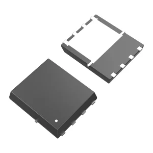
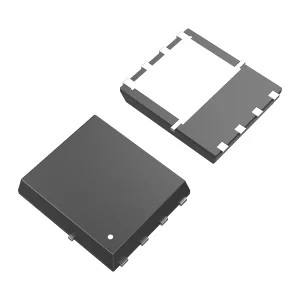
Premium low-to-medium voltage N-Channel MOSFET products optimized for high efficiency, thermal performance, and strict industry compliance.
Analyzing supply patterns, technical dynamics, and macro growth factors within modern power grid networks.
The global demand for high-efficiency N-Channel MOSFETs has surged exponentially. Industrial systems, electric vehicles (EVs), and smart grids are expanding rapidly. This pushes the semiconductor supply chain to deliver high-performance, cost-effective alternatives. System designers are looking beyond traditional Tier-1 fabs to secure component supply.
Modern power topologies require lower R_DS(on) and gate charge values. In the Asia-Pacific region, centers like Shenzhen and Hong Kong serve as major sourcing hubs. Distributors like Hongkong Olukey Industry bridge the gap between chip designers and high-volume manufacturers, ensuring stable lead times.
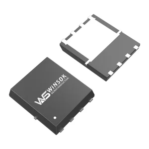
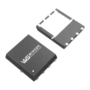
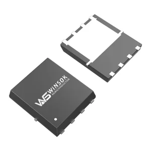
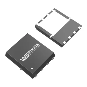
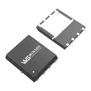
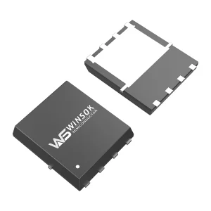
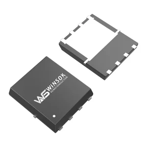
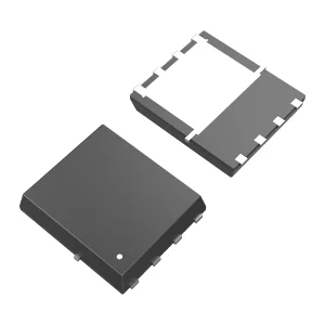
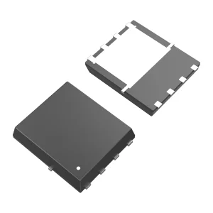
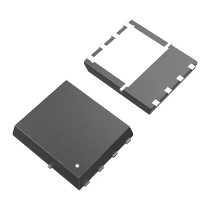
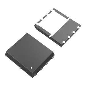
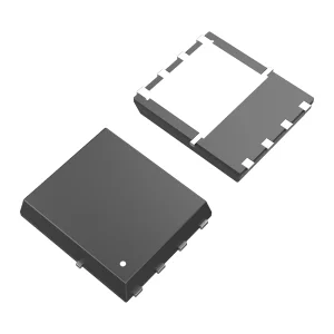
Standard packaging like TO-220 and TO-252 is still widely used. However, DFN packages like DFN5x6-8 are becoming the new industry standard. They significantly reduce parasitic inductance, lower thermal resistance, and minimize board footprint. This makes them ideal for dense consumer electronics and compact industrial power supplies.
How advanced trench technology and packaging optimization drive high-density electrical conversion efficiency.
Modern silicon designs rely on trench-gate technology to pack more conduction channels onto a single die. This structure increases the channel perimeter per unit area, reducing the overall on-state resistance (R_DS(on)) without growing the silicon footprint. This tech minimizes conduction losses, making it ideal for high-current applications.
Additionally, engineers focus on lowering gate-to-drain charge (Q_gd). This reduces switching losses, allowing designers to operate power stages at higher frequencies. Operating at higher frequencies enables the use of smaller, lighter passive components, like inductors and capacitors.
Even the most efficient silicon produces heat under heavy current loads. Packages like the DFN5x6-8 address this with a large exposed thermal pad on the underside of the package. This design provides a low-resistance path to the system PCB, dissipating heat much more effectively than leaded packages.
Lowering junction-to-case thermal resistance (R_thJC) prevents localized hotspots. This directly improves system reliability and extends the lifespan of components in demanding setups like industrial motor controllers and DC-DC converters.
Deploying high-performance power devices across various sectors, from industrial machinery to consumer devices.
High-voltage N-Channel MOSFETs (such as 100V, 120V, and 150V models) are critical in motor control, robotics, and industrial SMPS. Robust avalanche energy ratings (UIS) protect circuits against inductive voltage spikes from electric motors.
5G base stations and data center servers require high power density in compact spaces. N-Channel devices in DFN packages optimize sync rectification stages, reducing energy waste and ensuring constant service uptime.
Low-voltage MOSFETs (15V to 30V) are vital for power delivery in mobile devices, smart home products, and laptops. Minimizing gate charge allows circuits to switch efficiently, extending battery life and reducing operating temperatures.





We are a solution provider focused on total components packages for electronic products. Our core product lines include: WINSOK MOSFETs, Cmsemicon MCUs, and custom PCBA circuit board development.
Our products are widely used in automotive electronics, industrial control, green energy systems, smart medical equipment, 5G infrastructure, IoT networks, and smart home appliances. We leverage our close partnerships with global factories to supply advanced electronic components across the Asia-Pacific region.
By offering dedicated technical support and reliable supply chains, we help manufacturers improve product quality and optimize development cycles.


With years of experience in electronic component distribution, we build relationships on quality and service. We act as a trusted partner, helping domestic and international high-tech companies source reliable components.
WINSOK MOSFET's product voltages span a wide medium-and-low range: 15V, 20V, 30V, 40V, 60V, 80V, 100V, 120V, 150V, 200V, 250V, 300V, 400V, 500V, 600V, and 650V. We support over 40 package types (DFN3X3-8, DFN5X6-8, TO-252, TO-263, SOP-8, SOT-23, TO-220, etc.) and over 600 unique models, providing comprehensive coverage for your application needs.
By pairing WINSOK's power devices with Cmsemicon MCU's microcontrollers, we deliver complete, integrated system designs. We are committed to growing the global semiconductor market alongside our customers and suppliers.
Common questions from hardware engineers and procurement managers regarding design, sourcing, and cross-referencing.
WINSOK MOSFETs are designed to match standard specifications and pin layouts. They provide drop-in replacements for common industry models, including the AON series (e.g., AON6264C, AON6276) and TI's CSD series. This allows engineers to drop them into existing layouts without needing to redesign the board, providing a reliable alternative during supply shortages.
Key parameters include R_DS(on) to minimize conduction losses, and gate charge (Qg/Qgd) to limit switching losses. The body diode's reverse recovery charge (Qrr) is also important to prevent voltage spikes, while package thermal resistance (R_thJC) ensures proper heat dissipation.
The DFN5x6-8 package reduces package parasitic inductance and resistance. It features an exposed thermal pad that conducts heat directly to the PCB ground plane, providing better thermal performance than TO-252 in a smaller footprint.
We implement strict quality controls and inspect components in our testing facilities. Our partnerships with original factories ensure traceablity and consistent performance across production runs.
Broad range of package options, from low-voltage devices to medium-voltage silicon, designed for complex electronic applications.
 Olukey