
HONGKONG Olukey INDUSTRY CO., LIMITED is an industry-leading component solution provider, specializing in providing comprehensive, advanced power semiconductor architectures for global OEMs, ODMs, and EMS corporations. Our core business ecosystem is built upon three pillar product lines: WINSOK MOSFETs, Cmsemicon MCUs, and customized PCBA circuit board layout design and system-level development.
Operating as a critical bridge between silicon fabrication and application deployment, we specialize in high-efficiency design-in support for multiple sectors. Currently, our state-of-the-art product portfolios are deployed within automotive infotainment and drivetrains, industrial computing, military and aerospace modules, smart energy storage systems, medical instrumentation, 5G base stations, the Internet of Things (IoT), intelligent appliance controllers, and consumer products. By aligning with top-tier semiconductor fabs and leveraging our direct factory pipelines, we deliver robust pricing, supply security, and localized technical engineering support.
Combining strict raw-material qualification with design-to-spec flexibility, we enable engineering teams to achieve higher power density, lower thermal overhead, and sustained cost-efficiency.
WINSOK MOSFET voltage range covers low and medium-to-high voltage spectrums: 15V, 20V, 30V, 40V, 60V, 80V, 100V, 120V, 150V, 200V, 250V, 300V, 400V, 500V, 600V, and 650V. With over 600 unique part numbers, we provide drop-in equivalents to tier-one global silicon manufacturers.
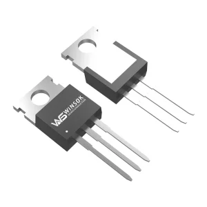
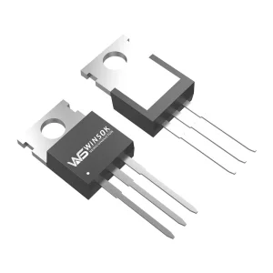
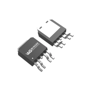
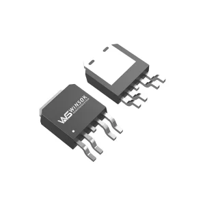
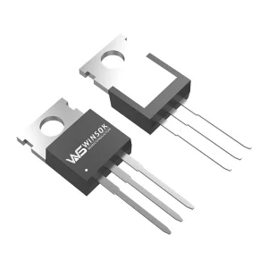
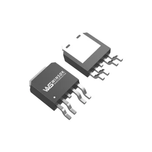
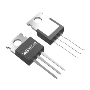
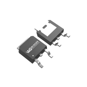
We supply a diverse array of over 40 package types, including high-density DFN3X3-8, DFN5X6-8, TO-252 (DPAK), TO-263 (D2PAK), SOP-8, SOT-23, and TO-220. This selection allows design engineers to optimize layout footprint size versus thermal dissipation limits.
Beyond simple power transistors, our partnership with Cmsemicon allows us to supply microcontrollers alongside your power stages. This co-design of MCU and MOSFET minimizes EMI issues, reduces development cycle durations, and optimizes the system bill of materials (BOM).
The global power semiconductor market is undergoing a significant transition. Driven by energy efficiency regulations, electrification, and high-frequency switching requirements, demand for traditional Transistor Outline (TO) packages like the TO-220 and TO-252 remains high. These packages offer mechanical stability and excellent thermal management compared to smaller surface-mount alternatives.
In heavy industrial zones across North America, Europe, and Asia-Pacific, legacy systems require drop-in replacements that can handle high currents and manage thermal dissipation under heavy workloads. Industrial motors, central grid solar invertors, and switch-mode power supplies (SMPS) continue to rely on the TO-220 package for its capability to mount onto external heatsinks. This keeps the junction temperature ($T_j$) within safe operating limits during continuous use.
At OLUKEY Industry, we analyze these global market dynamics. We ensure that our WINSOK TO-packaged silicon portfolio meets both existing parameters and upcoming efficiency standards, such as the 80 Plus Titanium standard for server power supplies and AEC-Q101 automotive requirements.

China’s semiconductor ecosystem offers high integration, bringing together raw silicon processing, lead-frame fabrication, packaging, and functional testing in close proximity. This geographic concentration of the supply chain allows WINSOK’s state-of-the-art facilities to operate efficiently and respond quickly to market needs.
Our manufacturing facilities benefit from advanced raw material sourcing, automated wafer testing, and high-volume assembly lines. While traditional supply lines can experience long lead times during geopolitical or market disruptions, our logistics network maintains safety stock levels in regional warehousing hubs. By using copper clip bonding and automated optical inspections (AOI), we achieve low defect rates (measured in PPB) while maintaining competitive manufacturing costs.
This operational model allows OLUKEY Industry to offer stable lead times (typically 4–6 weeks for non-stocked components) compared to the longer timelines of 16-26 weeks often found elsewhere in the industry. This efficiency helps clients maintain continuous production schedules.

From the cold environment of high-latitude telecommunication stations to the hot environment of EV motor compartments, our TO-252 and TO-220 devices are optimized for real-world stress conditions.
In Electric Vehicles (EVs) and Hybrid EVs, low-voltage DC-DC converters step down the high-voltage battery pack (400V/800V) to feed 12V/48V subsystem channels. Our WSR200N08 (80V 200A TO-220) provides low $R_{DS(on)}$ to reduce thermal losses in synchronous rectification circuits, ensuring stable power delivery for vehicle control units.
Brushless DC motors used in logistics systems require drivers that can handle high current spikes during startup. Using N&P-channel pairings in a TO-252 package, such as the WSF6012 N&P-Channel, helps reduce component count in H-bridge designs while maintaining durability under high motor kickback voltages.
Micro-inverters require power MOSFETs with stable breakdown voltages ($V_{(BR)DSS}$) and low gate charge ($Q_g$) to minimize switching losses at high frequencies. Our medium-voltage WSR140N12 (120V 140A TO-220) provides stable efficiency in solar boost stages, even during temperature variations in outdoor installations.
Power architectures are moving toward higher switching speeds, lower on-resistance, and better thermal performance. Here is our product roadmap for the coming years.
Developing sub-1mΩ Trench MOSFETs in standard TO-220 and TO-263 packages. This design aims to reduce conduction losses in high-current battery protection boards without needing complex parallel circuits.
Moving from traditional wire-bonding to copper clip-bonding inside TO-252 and DFN variants. This update reduces package resistance, lowers stray inductance, and improves thermal transfer to the system PCB.
Integrating driver ICs directly with the MOSFET power stage. By combining WINSOK’s power silicon with Cmsemicon's control logic, we aim to deliver compact, intelligent power modules for industrial automation.


Operating as an international partner requires strict compliance with environmental regulations and quality standards. Our product range is compliant with RoHS and REACH, and we verify that all raw materials are sourced from conflict-free regions.
Through our sales networks in Europe, North America, and the Asia-Pacific region, we provide direct access to application engineering support (FAE). When a customer experiences an unexpected failure under load (e.g., during avalanche testing or high $dv/dt$ conditions), our laboratories can perform cross-sectional failure analysis, package decapsulation, and curve tracing.
We also provide simulation files, including SPICE models, to assist design teams in conducting thermal and electromagnetic analysis before creating physical prototypes. This support helps shorten time-to-market and improves system reliability.

Deep engineering answers regarding thermal dissipation, parasitics, and component substitution guidelines.

 Olukey