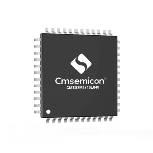
Explore our primary selection of high-efficiency, low Rds(on) power switch components designed to optimize solar conversion efficiencies.


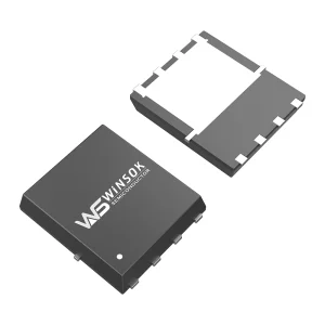
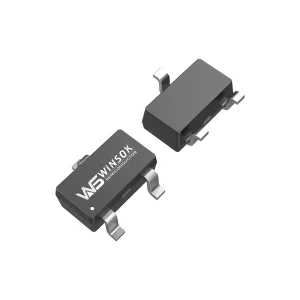
In the rapidly accelerating clean energy sector, the efficiency of solar energy systems relies heavily on the performance of solid-state semiconductor switching devices. In a photovoltaic (PV) setup, the **solar inverter** acts as the crucial link, converting raw DC power from the panels into stable, grid-compliant AC electricity.
As inverter designs shift from traditional centralized typologies towards decentralized architectures, such as **string inverters** and **microinverters**, the demand for high-efficiency, reliable power MOSFETs has surged. These topologies require power components with minimal switching and conduction losses to achieve over 98% efficiency. Finding high-performance **equivalent MOSFETs** that provide drop-in replacements for industry-standard parts has become a top priority for procurement managers and design engineers globally.
Modern solar inverters run at high frequencies to shrink the size of passive components like inductors and capacitors. However, higher switching frequencies increase switching losses ($P_{sw}$). To mitigate this, next-generation MOSFET designs focus on minimizing key parameters:
When cross-referencing equivalents for well-known brands like Infineon, ON Semiconductor, or STMicroelectronics, engineers must examine not only the voltage ($V_{DS}$) and current ($I_D$) limits but also the gate threshold voltage ($V_{GS(th)}$) and reverse recovery time ($t_{rr}$) of the body diode.
WINSOK MOSFET addresses these design needs by offering over 600 models across more than 40 package types. Their product portfolio spans a broad range of voltages including **15V, 20V, 30V, 40V, 60V, 80V, 100V, 120V, 150V, 200V, 250V, 300V, 400V, 500V, 600V, and 650V**. Below is a comparative overview of common solar equivalent parameter mappings:
| Target Voltage Class | Standard Package | Key Parameter Focus | WINSOK Direct Equivalent Options |
|---|---|---|---|
| 60V - 100V (Low-Side MPPT Boost) | DFN5x6-8L / TO-252 | Ultra-low $R_{DS(on)}$, Low $Q_{gd}$ | WSD100N15DN56G, WSD40120DN56 Series |
| 150V - 200V (Intermediate Bus Stage) | TO-220-3L / TO-252 | High Avalanche Ruggedness (UIS) | WSR135N15, WSF12N15 Series |
| -20V to -60V (P-Channel Driving/Protection) | DFN3x3 / SOP-8L | Logic level gate drive, Stable $V_{GS(th)}$ | WSD30L40DN33, WSR88P06 Series |
As a global solution provider, HONGKONG Olukey INDUSTRY CO., LIMITED specializes in delivering complete electronic component solutions. Their main product lines focus on:
Olukey Industry leverages original-factory relationships and direct agency access to distribute components that support critical applications in automotive electronics, military electronics, industrial automation, and renewable energy systems.
Procurement teams face ongoing challenges from market volatility, component obsolescence, and extended lead times from tier-one manufacturers. The solar sector requires long-term planning, where component lead times can make or break production schedules.
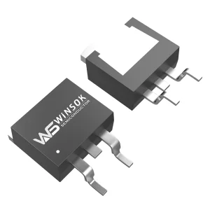
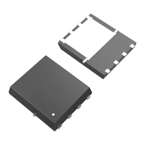
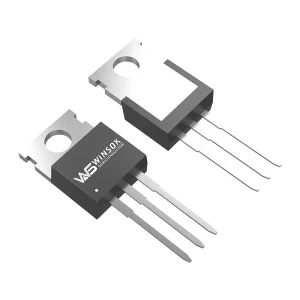
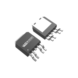
In this environment, relying on single-source components introduces significant risk. Developing qualified, pin-to-pin, and functionally equivalent bill-of-materials (BOM) alternatives is key to building a resilient supply chain. Standardizing packages like DFN5X6-8, DFN3X3-8, TO-252, TO-263, SOP-8, SOT-23, and TO-220 allows manufacturers to swap components easily without redesigning their PCBs.
The modernization of China's semiconductor manufacturing has reshaped global electronics procurement. Under Industry 4.0 initiatives, domestic wafer fabrication and packaging lines utilize high levels of automation and advanced process control.
For brands like WINSOK, this integration provides dual advantages:
Power requirements vary across residential, commercial, and utility-scale solar projects. Each scenario dictates distinct electrical requirements for MOSFET switches:
Microinverters process power at the individual panel level, converting 30V-60V DC into AC. High efficiency is critical, as these units are installed directly beneath panels and operate in warm environments. Small form-factor packages like DFN3X3-8 and DFN5X6-8 N-channel MOSFETs are preferred here because their low gate charge reduces switching losses at higher frequencies.
Operating at higher voltages and currents, string inverters require robust switches like TO-220-3L and TO-263-2L packages. These devices must handle continuous thermal cycling. Low $R_{DS(on)}$ is essential to limit heat build-up under full load, reducing the size of required heatsinks and cooling systems.
Modern solar setups are increasingly paired with battery storage. Bidirectional DC-DC converters manage power flow between PV arrays, batteries, and the grid. Using dual N-channel or combined N+P-channel MOSFET packages (such as the WST2038 or WSF3012) allows designers to build compact synchronous rectification circuits, saving board space and improving charging efficiency.

Providing global distribution and comprehensive design-in support.

Automated silicon manufacturing processes ensure reliable component parameters.

Parametric testing ensures compliance with target specs.
By partnering with HONGKONG Olukey INDUSTRY CO., LIMITED, clients gain access to a resilient supply chain, cost-competitive alternatives, and technical design support.
Our engineering team ensures all cross-referenced equivalents match or exceed the target specification metrics, backed by full parametric test documentation.
Offering packaging form factors from SOT-23 up to high-power TO-220-3L and DFN5X6-8L configurations to fit varying board space limitations.
Receive direct support from application engineers, including reference designs using WINSOK MOSFETs and Cmsemicon MCUs for integrated power stages.



Substituting power switches in solar inverter systems requires careful review of all technical parameters. Simple pin-compatibility is not enough; the switching performance of the replacement device must align with the gate driver's characteristics to avoid efficiency loss or premature failure.
Ensure the replacement MOSFET's breakdown voltage ($V_{DSS}$) equals or exceeds the original component's rating. The $R_{DS(on)}$ should be checked at the specific gate drive voltage ($V_{GS} = 4.5\text{V}$ or $10\text{V}$) used in the system, as some logic-level MOSFETs behave differently under standard driving voltages.
Input capacitance ($C_{iss}$) dictates the current required from the gate driver to charge the gate to the target voltage. If $C_{iss}$ is significantly higher than the original device, the gate driver may overheat or experience slower turn-on times, increasing switching losses. $C_{oss}$ (output capacitance) and $C_{rss}$ (reverse transfer capacitance) should also be matched to prevent high-frequency oscillations during switching transitions.
Evaluate the package's thermal resistance to the case ($R_{\theta JC}$) and to the ambient air ($R_{\theta JA}$). Advanced surface-mount packages, like the DFN5x6, offer thermal performance comparable to larger through-hole designs (like TO-220) while reducing parasitic inductance. Ensure the device operates well within its Safe Operating Area (SOA), especially during startup or fault conditions.

Clear answers to common questions about solar inverter MOSFET cross-referencing, purchasing, and distribution.
Explore our secondary catalog options, highlighting complementary products, microcontroller solutions, and high-performance power configurations.

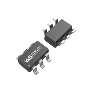
 Olukey