How advanced silicon chemistry and precision package engineering ensure system uptime while easing supply chain blockages.
The explosive growth of Battery Energy Storage Systems (BESS) across residential, commercial, and utility-scale grids demands power switching hardware of unmatched integrity. In these topologies, the MOSFET acts as the fundamental gatekeeper of safety, managing active cell balancing, protection, and DC-DC power conversion. Finding a reliable OEM MOSFET Equivalent is not merely about finding a footprint match; it requires matching transient capabilities, gate charge dynamics, and thermal signatures.
For engineering departments and global buyers, standardizing on cross-compatible, high-performance replacements is the key to decoupling development loops from manufacturing lead times. By utilizing optimized medium-to-low voltage MOSFET equivalents, manufacturers can guarantee system design resilience against volatile raw component markets without suffering degradation in efficiency or power density.

A detailed look at replacement parameters: how to secure identical thermal performance and efficiency curves.
| Typical BESS Function | Reference OEM Parts | WINSOK Equivalent Solution | Voltage / Current Range | Primary Package Types | Key Performance Metrics |
|---|---|---|---|---|---|
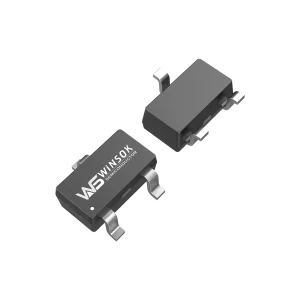
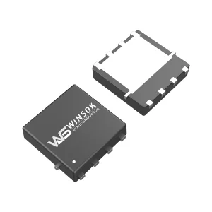
| Low-Voltage BMS Protection | BSC050N03MSG, CSD17327Q5A | WSD3072DN33 | 30V / 72A | DFN3X3-8L | Low $R_{DS(ON)}$, minimized gate charge ($Q_g$) |
| Medium-Voltage Inverter DC-DC | TPH4R803PL, TPH3R203NL | WSF12N15 | 150V / 10A | TO-252-2L | Exceptional avalanche ruggedness, low parasitic $C_{iss}$ |
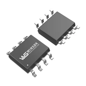
| Active Cell Balancing / Switch | AO4425, FDS4675, Si4401FDY | WSD30L40DN33 | -30V / -40A | DFN3X3-8L | Highly stable P-channel threshold, low driving loss |
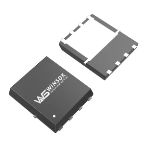
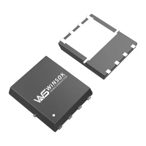
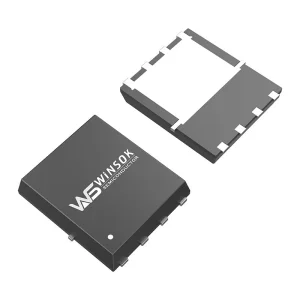
| High-Current Power Distribution | CSD17307Q5A, PJQ5410 | WSD30150ADN56 | 30V / 145A | DFN5X6-8 | Extremely low package resistance, superior source-clip binding |
| High-Voltage Auxiliary Supplies | Si4401FDY, STS10P4LLF6 | WSD50P10DN56 | -100V / -34A | DFN5X6-8 | Excellent EMI margin, stable switching trajectory |
Selecting the correct equivalence profile involves validating the thermal impedance ($R_{\theta JC}$), maximum junction temperature ($T_j$), and the Safe Operating Area (SOA) curves to ensure flawless performance under system fault states.
Deploying WINSOK MOSFETs and Cmsemicon MCUs across the energy generation, transmission, and usage landscape.
Modern home battery packs require compact, efficient power switches to manage safe discharge cycles. WINSOK's low RDS(on) DFN and SOP-8 pack variations limit board heat dissipation, saving precious cooling space and extending lifetime metrics in sealed IP-rated enclosures.
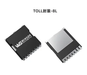
Megawatt-class installations depend on reliable components to handle peak shaving and frequency regulation duties. High-current packages like TOLLA-8L and TO-263 provide the needed robust package terminal current-handling capacity to withstand heavy transient loads.
Renewable power sources use bi-directional DC-DC blocks to shift energy between PV arrays and lithium battery banks. Fast-switching N-channel MOSFET devices lower switching losses ($E_{on}$ and $E_{off}$) to yield overall conversion efficiencies greater than 98%.

Leveraging deep industrial ecosystems in the Asia-Pacific region, Hongkong Olukey Industry Co., Limited ensures supply continuity through advanced manufacturing agreements with top-tier silicon foundries and package centers. Our production lines utilize automated Optical Inspection (AOI), high-throughput parametric testing, and rigorous burn-in steps to maintain near-zero PPM defect ratios.
This localized packaging and testing agility translates to immediate lead-time reductions from standard industry cycles of 26-52 weeks down to just 6-8 weeks. Furthermore, this concentration of resources lowers structural unit cost, passing significant savings onto BESS system designers and assembly houses.



Where silicon is headed and how BESS systems will transition into next-generation power structures.
The roadmap for BESS-grade power switches focuses on two parallel tracks: the ongoing improvement of silicon (Si) superjunction structures and the targeted adoption of Wide Bandgap (WBG) materials like Silicon Carbide (SiC) and Gallium Nitride (GaN).
Our research and manufacturing focus remains heavily invested in shrinking the specific RDS(on) per unit area of our silicon trench geometries. This allows us to pack high-current capability into standard DFN package types. For high-density systems, this trend drives the replacement of older TO-220 devices with low-parasitic surface-mount packages like DFN5X6-8 and TOLLA-8L.
Additionally, as cell pack voltages push from 48V upwards to 400V and 800V to reduce transmission losses, we are actively expanding our portfolio of high-voltage MOSFET switches (up to 650V). This expansion targets auxiliary power circuits and dynamic protection switches, giving BESS builders a reliable roadmap for the next decade of power engineering.

Meeting strict international regulatory frameworks and logistics requirements for top-tier energy storage manufacturers.
All WINSOK products are fully compliant with RoHS 2.0 and REACH environmental directives, ensuring lead-free and halogen-free manufacturing processes. This is critical for European and North American market entries, where compliance documentation is required for import custom approvals.
For systems that require enhanced safety and stability, our manufacturing facilities operate under IATF 16949 quality guidelines. Selected MOSFET ranges feature design processes derived from automotive AEC-Q101 standards, delivering low failure rates during lifetime deployments.
Hongkong Olukey Industry Co., Limited manages buffer stocking facilities across primary economic hubs in the Asia-Pacific region. This geographic layout safeguards shipments against maritime shipping delays, ensuring that BESS manufacturing lines remain running.
HONGKONG Olukey INDUSTRY CO., LIMITED: Your Trusted Partner in Power Semiconductors.
HONGKONG Olukey INDUSTRY CO., LIMITED is a comprehensive solution provider focusing on the overall layout and engineering of electronic product components. The company's main offerings span three critical product lines: WINSOK MOSFETs, Cmsemicon MCUs, and PCBA circuit board solution development. This wide engineering baseline allows Olukey to supply not just isolated components, but complete, integrated sub-system layouts for complex projects.
At present, Olukey Industry's components are widely deployed in automotive electronics, military systems, smart industrial controls, new energy ecosystems, smart healthcare hardware, 5G networking blocks, the Internet of Things, smart home controls, and consumer electronics. Based in the Asia-Pacific market, we leverage our partnerships with major original wafer plants to provide customers with advanced, high-tech components, backed by comprehensive support services.
Our core operating values – Pragmatism, Win-win, Service, and Responsibility – drive our teams to constantly reinforce service quality. We work closely with our supply chain partners to explore new market frontiers and contribute to the growth of the semiconductor sector.

Answering common engineering and procurement questions regarding MOSFET cross-referencing and BESS designs.
 Olukey