Olukey
1 / 1
| Symbol | Parameter | Condition | Rating | Unit |
|---|---|---|---|---|
| Common Ratings | ||||
| VDSS | Drain-Source Voltage | - | 40 | V |
| VGSS | Gate-Source Voltage | - | ±20 | V |
| TJ | Maximum Junction Temperature | - | 150 | °C |
| TSTG | Storage Temperature Range | - | -55 to 150 | °C |
| IS | Diode Continuous Forward Current | TA=25°C | 11.4 | A |
| ID | Continuous Drain Current | TA=25°C | 22 | A |
| TA=70°C | 22 | |||
| IDM | Pulse Drain Current Tested | TA=25°C | 88 | A |
| PD | Maximum Power Dissipation | TC=25°C | 25 | W |
| TC=70°C | 10 | |||
| RqJL | Thermal Resistance-Junction to Lead | Steady State | 5 | °C/W |
| RqJA | Thermal Resistance-Junction to Ambient | t ≤ 10s | 45 | °C/W |
| Steady State | 90 | |||
| IAS | Avalanche Current, Single pulse | L=0.5mH | 28 | A |
| EAS | Avalanche Energy, Single pulse | L=0.5mH | 39.2 | mJ |
| Symbol | Parameter | Test Conditions | Min. | Typ. | Max. | Unit | |
|---|---|---|---|---|---|---|---|
| Static Characteristics | |||||||
| BVDSS | Drain-Source Breakdown Voltage | VGS=0V, IDS=250μA | 40 | - | - | V | |
| IDSS | Zero Gate Voltage Drain Current | VDS=32V, VGS=0V | - | - | 1 | μA | |
| TJ=85°C | - | - | 30 | ||||
| VGS(th) | Gate Threshold Voltage | VDS=VGS, IDS=250μA | 1.2 | 1.8 | 2.5 | V | |
| IGSS | Gate Leakage Current | VGS=±20V, VDS=0V | - | - | ±100 | nA | |
| RDS(ON) | Drain-Source On-state Resistance | VGS=10V, IDS=14A | - | 6.8 | 7.8 | mΩ | |
| VGS=4.5V, IDS=12A | - | 9.0 | 11 | ||||
| Diode Characteristics | |||||||
| VSD | Diode Forward Voltage | ISD=1A, VGS=0V | - | 0.75 | 1.1 | V | |
| trr | Reverse Recovery Time | ISD=20A, dISD/dt=100A/μs | - | 23 | - | ns | |
| Qrr | Reverse Recovery Charge | - | 13 | - | nC | ||
| Dynamic Characteristics | |||||||
| RG | Gate Resistance | VGS=0V, VDS=0V, F=1MHz | - | 2.5 | - | Ω | |
| Ciss | Input Capacitance | VGS=0V, VDS=20V, Frequency=1.0MHz | - | 1370 | 1781 | pF | |
| Coss | Output Capacitance | - | 317 | - | |||
| Crss | Reverse Transfer Capacitance | - | 96 | - | |||
| td(ON) | Turn-on Delay Time | VDD=20V, RL=20Ω, IDS=1A, VGEN=10V, RG=6Ω | - | 13.8 | - | ns | |
| tr | Turn-on Rise Time | - | 8 | - | |||
| td(OFF) | Turn-off Delay Time | - | 30 | - | |||
| tf | Turn-off Fall Time | - | 21 | - | |||
| Gate Charge Characteristics | |||||||
| Qg | Total Gate Charge (10V) | VDS=20V, VGS=10V, IDS=6A | - | 23 | 28 | nC | |
| Qg | Total Gate Charge (4.5V) | VDS=20V, VGS=4.5V, IDS=6A | - | 22 | - | ||
| Qgth | Threshold Gate Charge | - | 2.6 | - | |||
| Qgs | Gate-Source Charge | - | 4.7 | - | |||
| Qgd | Gate-Drain Charge | - | 3 | - | |||
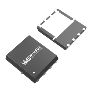
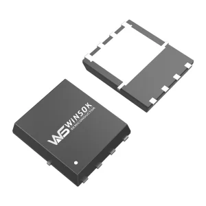
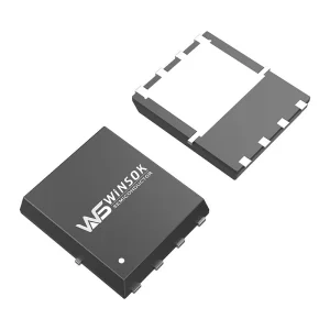
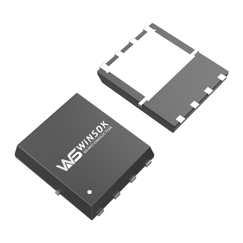
The WSD4098DN56 is a high-performance trench Dual N-Channel MOSFET designed primarily for synchronous buck converter applications, load switches, and high-frequency point-of-load systems.
It features a drain-source breakdown voltage rating of 40V, making it highly suitable for 12V to 24V power systems.
It provides excellent on-state resistance, with a typical RDS(ON) of 6.8 mΩ at VGS=10V and 9.0 mΩ at VGS=4.5V, minimizing power dissipation.
Yes, the WSD4098DN56 can be cross-referenced with the AOS AON6884 model.
Yes, this device is 100% compliant with RoHS and Green Product requirements, featuring full function reliability approval.
It is widely applied in e-cigarettes, wireless chargers, drone motors, car chargers, medical devices, small household appliances, and other digital consumer electronics.