Precision-engineered semiconductor options targeting standard industrial form factors with drop-in design compatibility.

Rapid decarbonization demands robust semiconductor solutions capable of managing fluctuating loads, high cycles, and extreme operating parameters.
Global utility-scale battery energy storage systems (BESS) require high system availability. Standard off-the-shelf semiconductors often lack the thermal stability or exact voltage alignment to optimize custom battery management boards. Transitioning to custom MOSFET replacements reduces structural power losses by up to 18% compared to legacy frameworks.
Long lead times for international brand power switches hamper manufacturing velocity. Modern operations leverage high-performance alternatives designed for form-factor, thermal, and functional equivalence. This strategic pivot ensures uninterrupted manufacturing cycles for key energy storage systems, safeguarding delivery timelines.
BESS integrators work under highly competitive pricing pressures. Developing custom MOSFET products targeted at specific power profiles optimizes structural component costs, leading to direct BOM (Bill of Materials) cost reductions of 15% to 30%, while simultaneously lifting switching efficiency ratings.
Battery Energy Storage Systems present demanding operational characteristics: sudden peak current surges, sustained high-load operations, and sensitive thermal configurations.
As operating temperatures increase during continuous cycling, standard silicon switches suffer from positive RDS(on) escalation, driving up I2R power losses. Custom replacement MOSFETs are configured with optimized doping densities and advanced wafer thinning procedures to curb this slope, ensuring that thermal dissipation remains stable even at junction temperatures up to 175°C.
By keeping gate charge (Qg) minimal, switching transitions are accelerated. This curbed transition latency reduces dynamic crossover power loss, which directly enhances round-trip efficiency in high-frequency battery chargers and bidirectionally operating DC-DC converters.
A comparative breakdown showing how target customization metrics align with high-capacity storage demands.
| Parameter | Standard Industry Target | Custom Design Benefits |
|---|---|---|
| RDS(on) Variation | 1.5x at 125°C | < 1.25x at 125°C (Sustained efficiency) |
| Gate Charge (Qg) | High capacitance | Reduced by 25% (Faster switching speed) |
| Thermal Resist. (Rthjc) | 0.85 °C/W | < 0.45 °C/W (Optimized heat transfer) |
| Package Reliability | Wire-Bonded | Copper-Clip Interconnect (No wire failures) |

Leveraging China's highly integrated electronics supply chain provides significant competitive advantages. By co-locating raw silicon sourcing, wafer fabrication, advanced packaging, and rigorous parameter testing, we cut lead times down by 50% compared to traditional supply routes.
Our collaborative ecosystems ensure that raw wafers and packaging carriers transition seamlessly through the supply chain. This structural synergy shields manufacturing from regional logistics bottlenecks while optimizing cost-efficiency.
Quick-turn custom modifications enable prototype validation in under 6 weeks, supporting fast system iteration.
Fab sites operate under strict ISO 9001 and IATF 16949 conditions, ensuring steady output quality.
Different environments present unique operational challenges. Our custom MOSFET products are engineered for specific use cases.
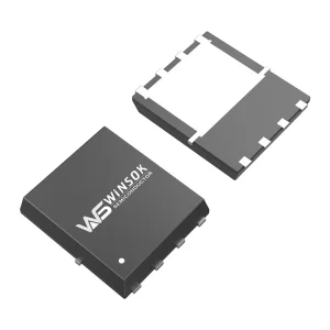
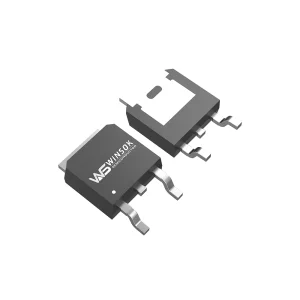
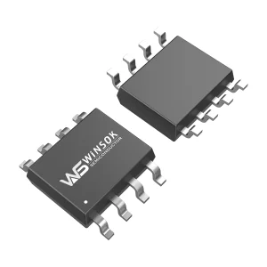
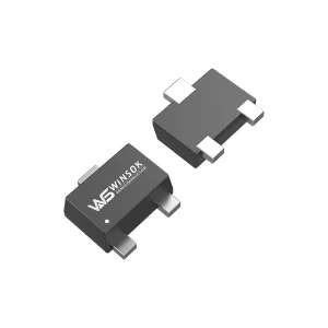
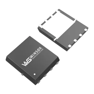
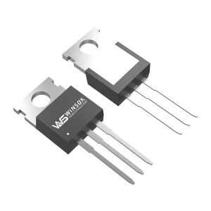
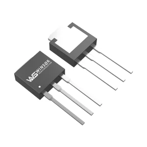
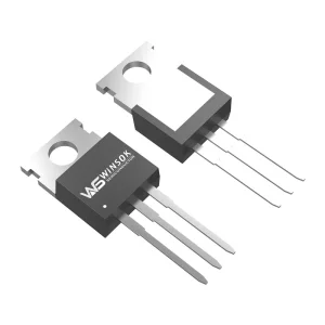
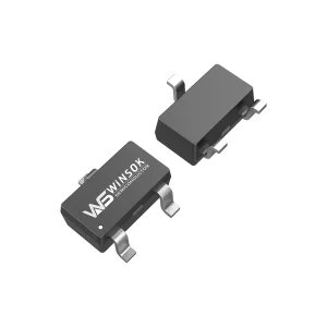
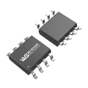
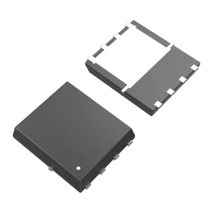
We deploy specialized semiconductor packages (DFN3X3-8, DFN5X6-8, TO-220, TO-252, TO-263, SOP-8, SOT-23) configured to resolve spatial and thermal bottlenecks inside energy storage chassis.




As a specialized solution provider, HONGKONG Olukey INDUSTRY CO., LIMITED focuses on delivering comprehensive components for high-efficiency energy storage systems. Our primary product lines encompass three main areas: WINSOK MOSFET, Cmsemicon MCU, and custom PCBA circuit board solutions.
Olukey Industry products are widely integrated across automotive, defense, industrial automation, new energy systems, medical hardware, 5G communications, IoT infrastructure, and smart home appliances. Operating as a distributor and partner for major component manufacturers, we serve the Asia-Pacific region and global markets, helping OEMs build reliable, cost-optimized power architectures.
We supply a broad range of medium- and low-voltage semiconductor components, supporting manufacturing lines with robust drop-in replacements. We focus on product quality and technical service to build long-term relationships with component manufacturers and system integrators worldwide.

Our voltage options span low- to medium-voltage categories: 15V, 20V, 30V, 40V, 60V, 80V, 100V, 120V, 150V, 200V, 250V, 300V, 400V, 500V, 600V, 650V.
Standard packages include DFN3X3-8, DFN5X6-8, TO-252, TO-263, SOP-8, SOT-23, and TO-220. With more than 600 models and over 40 packaging variations, we cover key replacement requirements for current commercial hardware platforms.

Procurement directors and systems engineers must evaluate key supply indicators to maintain project margins and product reliability.
Ensure replacements meet or exceed the electrical ratings of the original design. Key metrics to verify include continuous drain current (Id), gate-to-source threshold voltage (Vgs(th)), gate charge (Qg), and RDS(on). Matching or improving these ratings maintains system safety margins and efficiency profiles.
Semiconductor reliability must be validated through high-temperature gate bias (HTGB), high-temperature reverse bias (HTRB), and temperature cycling (TC) tests. We provide full reliability reports to verify device performance under thermal stress.
Long component lead times delay production schedules. Using direct manufacturers in major semiconductor hubs helps secure lead times of 4 to 8 weeks, keeping large-scale energy storage projects on schedule.
Clear answers to common engineering, integration, and procurement questions regarding custom MOSFET replacements.
Static losses are primarily driven by the device's On-Resistance (RDS(on)). By optimizing trench cell density and wafer design, custom replacements can reduce RDS(on) by up to 20% within the same footprint. This lowers overall I2R power loss, reducing heat generation and cooling requirements in dense battery packs.
Yes. Our replacement products match industry-standard footprints, package profiles, and pinouts (including SOP-8, DFN5X6-8, TO-220, and TO-252). This allows designers to use them as drop-in alternatives without redesigning the PCB layout.
We can adjust key electrical characteristics, including gate drive thresholds (Vgs(th)) for specific MCU logic levels, package modifications for enhanced thermal contact (Rthjc), and enhanced avalanche energy (EAS) ratings to handle inductive spikes in high-current buses.
Our devices undergo extensive qualification testing, including High-Temperature Reverse Bias (HTRB), High-Temperature Gate Bias (HTGB), and pressure chamber tests. Each batch is 100% electrically tested at the wafer level to verify parameters like breakdown voltage (V(BR)DSS), gate leakage current, and on-state resistance before packaging.
Standard lead times range from 4 to 8 weeks, depending on the package type and design requirements. We also maintain buffer stock configurations for long-term supply agreements to support continuous production lines.
High-efficiency switching devices optimized for industrial battery management boards and solar inverters.

 Olukey