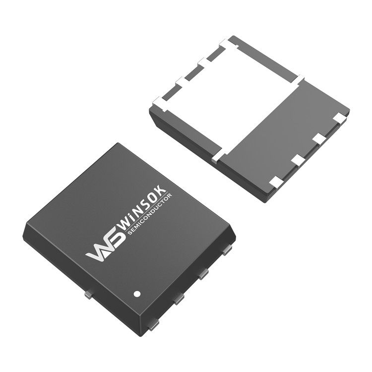
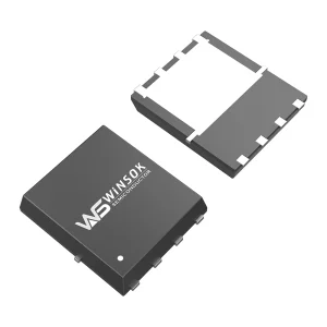
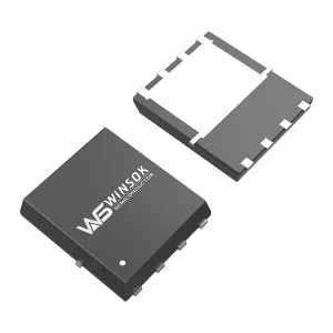
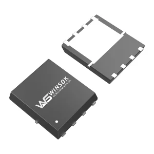
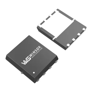
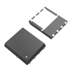
ODM WSD2090DN56 N-channel 20V 80A DFN5*6-8 WINSOK MOSFET Supplier, Distributor

Product Description

The WSD2090DN56 is the highest performance trench N-Ch MOSFET with extreme high cell density, which provides excellent RDSON and gate charge for most of the synchronous buck converter applications. The WSD2090DN56 meets the RoHS and Green Product requirement with 100% EAS guarantee and full function reliability approved.
Compatible / Cross Reference Part: AOS AON6572
Advanced high cell density Trench technology
Super Low Gate Charge
Excellent CdV / dt effect decline
100% EAS Guaranteed
Green Device Available

Absolute Maximum Ratings

Symbol Parameter Max. Units
VDSS Drain-Source Voltage 20 V
VGSS Gate-Source Voltage ±12 V
ID@TC=25℃ Continuous Drain Current, VGS @ 10V¹ 80 A
ID@TC=100℃ Continuous Drain Current, VGS @ 10V¹ 59 A
IDM Pulsed Drain Current note1 360 A
EAS Single Pulsed Avalanche Energy note2 110 mJ
PD Power Dissipation 81 W
RθJA Thermal Resistance, Junction to Case 65 ℃/W
RθJC Thermal Resistance Junction-Case 1 4 ℃/W
TJ, TSTG Operating and Storage Temperature Range -55 to +175

Electrical Characteristics

Symbol Parameter Conditions Min Typ Max Units
BVDSS Drain-Source Breakdown Voltage VGS=0V, ID=250μA 20 24 --- V
△BVDSS/△TJ BVDSS Temperature Coefficient Reference to 25℃, ID=1mA --- 0.018 --- V/℃
VGS(th) Gate Threshold Voltage VDS= VGS, ID=250μA 0.50 0.65 1.0 V
RDS(ON) Static Drain-Source On-Resistance VGS=4.5V, ID=30A --- 2.8 4.0 mΩ
VGS=2.5V, ID=20A --- 4.0 6.0
IDSS Zero Gate Voltage Drain Current VDS=20V, VGS=0V --- --- 1 μA
IGSS Gate-Body Leakage Current VGS=±10V, VDS=0V --- --- ±100 nA
Ciss Input Capacitance VDS=10V, VGS=0V, f=1MHZ --- 3200 --- pF
Coss Output Capacitance --- 460 ---
Crss Reverse Transfer Capacitance --- 446 ---
Qg Total Gate Charge VGS=4.5V, VDS=10V, ID=30A --- 11.05 --- nC
Qgs Gate-Source Charge --- 1.73 ---
Qgd Gate-Drain Charge --- 3.1 ---
tD(on) Turn-on Delay Time VGS=4.5V, VDS=10V, ID=30A, RGEN=1.8Ω --- 9.7 --- ns
tr Turn-on Rise Time --- 37 ---
tD(off) Turn-off Delay Time --- 63 ---
tf Turn-off fall Time --- 52 ---
VSD Diode Forward Voltage IS=7.6A, VGS=0V --- --- 1.2 V

Target Applications

Switch Power System Load Switch Electronic Cigarettes Drones Electrical Tools Fascia Guns PD (Power Delivery) Small Household Appliances

Frequently Asked Questions

What are the primary applications of the WSD2090DN56 MOSFET?
The WSD2090DN56 is designed for high-performance synchronous buck converter applications, load switches, power systems, drones, electronic cigarettes, electrical tools, fascia guns, PD, and small household appliances.
Is the WSD2090DN56 compatible with the AOS AON6572?
Yes, the WSD2090DN56 is a compatible cross-reference part to the AOS AON6572, offering extreme high cell density and superb performance in comparable circuit environments.
What is the RDS(ON) resistance of this MOSFET?
At VGS=4.5V, the typical RDS(ON) is 2.8mΩ (Max 4.0mΩ). At VGS=2.5V, the typical RDS(ON) is 4.0mΩ (Max 6.0mΩ).
What is the operating temperature range for the WSD2090DN56?
It features a wide operating and storage temperature range from -55 to +175 ℃, which ensures reliability in demanding environments.
Is this device environmentally compliant?
Yes, the WSD2090DN56 meets 100% of RoHS and Green Product requirements, with full function reliability approval and 100% EAS guarantee.
What is the maximum Drain-Source Voltage (VDSS) for this device?
The maximum Drain-Source Voltage (VDSS) for the WSD2090DN56 is rated at 20V.

Related Products