Explore our industry-validated MOSFET switches engineered for lower gate charge (Qg) and superior thermal dissipation.
Uninterruptible Power Supplies (UPS) form the backbones of modern IT infrastructure, data centers, industrial processing plants, and critical life-support medical systems. The primary metric governing a high-efficiency UPS system is its capability to transition power pathways seamlessly during mains dropouts with minimal switching loss ($P_{sw}$) and conduction loss ($P_{cond}$).
Historically, system architects relied on generic silicon power switches. However, modern high-power-density UPS designs demand custom silicon architectures. By optimizing parameters such as gate-source threshold voltage ($V_{GS(th)}$), reverse recovery time ($t_{rr}$), and package inductance, custom MOSFETs mitigate electromagnetic interference (EMI) and prevent fatal shoot-through scenarios in half-bridge or full-bridge inverter topologies.
At Hongkong Olukey Industry Co., Limited, we recognize that off-the-shelf semiconductors often introduce unwanted design trade-offs. We work intimately with system engineers to customize electrical profiles and package geometries, matching exact power architectures to optimize performance efficiency to 98% and beyond.

HONGKONG Olukey INDUSTRY CO., LIMITED is a leading solution provider focusing on the overall design and distribution of high-end electronic product components. Our core competencies span across three synergistic product segments: WINSOK MOSFETs, Cmsemicon MCUs, and end-to-end PCBA circuit board solutions.
Currently, Olukey Industry's advanced solutions are deployed globally across automotive electronics, aerospace, smart industrial control systems, new energy infrastructure (including photovoltaic inverters and wind generation), smart medical equipment, 5G telecommunication base stations, the Internet of Things (IoT) ecosystems, and consumer electronics.
By leveraging the strategic advantages of acting as global general agents of major original fabrication facilities, we are rooted firmly in the Asia-Pacific market. We support international manufacturers in achieving robust supply chains, minimizing design overheads, and deploying resilient electronic assemblies to market swiftly.




A heritage of high reliability, direct-to-fab logistics, and cross-disciplinary engineering excellence.
We use comprehensive high-quality services to provide customers with various types of advanced high-tech electronic components, assist manufacturers in producing high-quality products and provide comprehensive services. Over the years, the company has relied on reputation to survive, adhering to the tenet of "quality first, service first", and has established good cooperative relationships with many high-tech enterprises and original manufacturers at home and abroad.
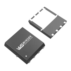
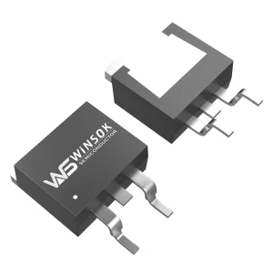
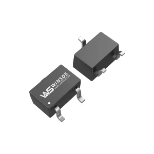
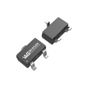
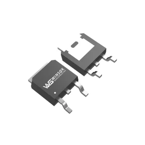
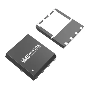
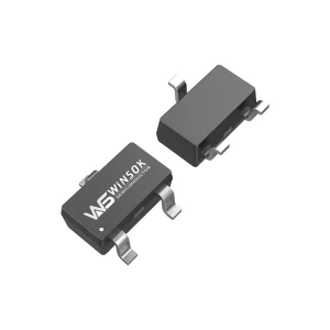
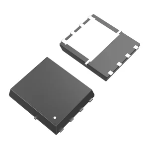
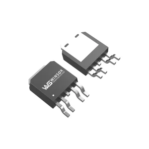
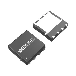
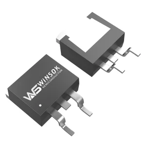
WINSOK MOSFET's product voltages are mainly medium and low voltage: 15V, 20V, 30V, 40V, 60V, 80V, 100V, 120V, 150V, 200V, 250V, 300V, 400V, 500V, 600V, 650V. The main packages include DFN3X3-8, DFN5X6-8, TO-252, TO-263, SOP-8, SOT-23, TO-220, etc. There are more than 600 models and more than 40 packages. Extensive coverage of medium-voltage and low-voltage MOSFET product lines on the market.
Relying on the advantages of global general agents of major original manufacturers, we are based on the Asia-Pacific market. Through active market development and effective resource integration, it has become one of the outstanding and fast-growing agents in the Asia-Pacific region. The company has many years of professional distribution experience. We offer unified designs comprising Cmsemicon MCUs and custom PCBAs to streamline power subsystem assembly.
Understanding the changing paradigms of global electronics trade, green power mandates, and supply chain security.

As data centers transition to hyperscale operations, the demand for high-efficiency UPS has grown exponentially. The transition towards 48V bus architectures in modern telecom racks and server clusters requires low $R_{DS(on)}$ MOSFETs in the 30V–100V range. System designers need switches that limit conduction loss while offering excellent ruggedness under cyclical peak-current demands.
Additionally, green energy mandates demand high efficiency at light-load conditions. In standard synchronous rectification setups, the parasitic body diode of the MOSFET is prone to high reverse recovery charges ($Q_{rr}$). If not managed, this creates voltage spikes that damage the device. Designers are sourcing custom-tuned internal gate resistors ($R_g$) and integrated Schottky barrier diodes (SBDs) to optimize switching speeds and suppress parasitic oscillations.
Comprehensive overview of available configurations optimized for various UPS charging and inverting circuits.
| Package Type | Common Voltage Ranges | Optimized Topology Stage | Key Engineering Highlights |
|---|---|---|---|
| DFN3X3-8 / DFN5X6-8 | 15V - 100V | Low-voltage DC-DC converters, Battery protection switch cards | Extremely low package parasitic inductance, flat leads for minimized PCB real estate. |
| TO-252 (DPAK) / TO-263 (D2PAK) | 30V - 150V | Synchronous Rectification, Buck-Boost controllers | High thermal dissipation area, handles continuous drain currents exceeding 80A. |
| SOP-8 / SOT-23 / SOT-323 | -12V to -100V (P-Channel), 20V to 60V (N-Channel) | Gate drive assistant circuits, auxiliary power rails, logic switching | Compact profiles for space-constrained signal routing. |
| TO-220 / TO-220F | 100V - 650V | Main Inverter switching bridges, PFC pre-regulators | Through-hole mounting permits simple heat-sink attachment for heavy thermal duty. |
By moving from legacy TO-220 units to customized DFN5X6-8 MOSFETs, developers can reduce power module volume by up to 60% while maintaining the same thermal performance.
Utilizing high-speed low gate charge switches in the secondary rectification stage improves conversion efficiency, removing the need for active cooling fans in small-to-medium UPS units.
By matching Cmsemicon microcontrollers with WINSOK MOSFETs, we deliver unified power subsystems with optimized gate drive voltage levels, ensuring clean turn-on states.
In the semiconductor industry, supply chain resilience is as critical as electrical efficiency. The cyclical nature of wafer allocations often leaves global UPS manufacturers exposed to lead-time variations. Sourcing custom power switches from a diversified, high-value partner ensures manufacturing continuity.
Hongkong Olukey Industry addresses this challenge through a multi-tiered supply architecture. Operating from the strategic logistical hub of Hong Kong and leveraging deep partnerships across the Asia-Pacific region, we secure long-term wafer allocations for our clients. Whether you require standard parts or custom packaging, we provide stable shipping schedules and buffer stocks.
This strategic foresight is complemented by our engineering capabilities. If an original manufacturer discontinues a product line, our research team can design and manufacture drop-in replacements with matching footprints and electrical characteristics, preventing costly redesigns.
All custom and distributed MOSFET lines undergo rigorous reliability screening prior to shipment. Every batch is qualified according to strict performance standards:

Anticipating next-generation technologies to help hardware designers stay ahead of the curve.
Traditional trench MOSFET structures face challenges in high-frequency applications due to elevated gate-to-drain capacitance ($C_{gd}$). This parameter limits switching transitions and increases losses. WINSOK's advanced shielded gate trench (SGT) technology resolves this by introducing a shielding electrode below the gate electrode.
This structural modification shields the gate from the drain potential, reducing $C_{gd}$ by up to 50% compared to standard trench designs. Consequently, the gate-drain charge ($Q_{gd}$) is minimized, enabling faster switching speeds and reduced switching energy ($E_{sw}$). Furthermore, SGT structures permit higher cell density, which reduces $R_{DS(on)}$ per unit area, supporting high current densities in compact packages.
While Wide Bandgap (WBG) technologies like Gallium Nitride (GaN) and Silicon Carbide (SiC) continue to advance, silicon-based power MOSFETs remain highly competitive. Their mature fabrication processes, cost efficiency, and proven reliability make them the preferred choice for low-to-medium voltage systems. Our design pipeline is structured to optimize silicon technology, ensuring these components meet modern efficiency requirements cost-effectively.
Answering critical questions on MOSFET selection, thermal management, and design integration in power subsystems.
Select from our comprehensive list of low, medium, and high-voltage power switches designed for industrial efficiency.

 Olukey