Olukey
1 / 1
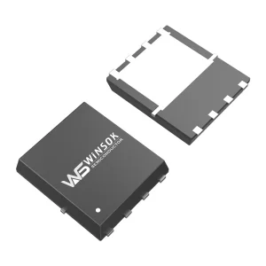
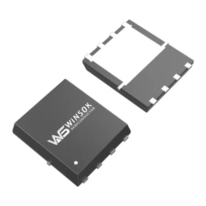
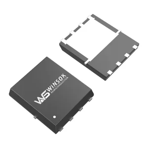
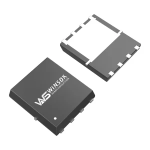
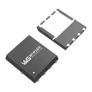
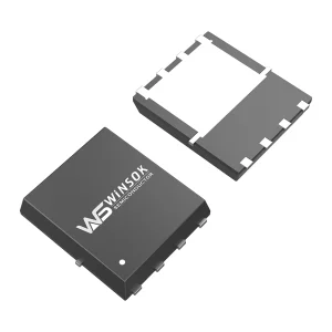
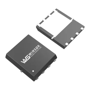
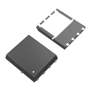
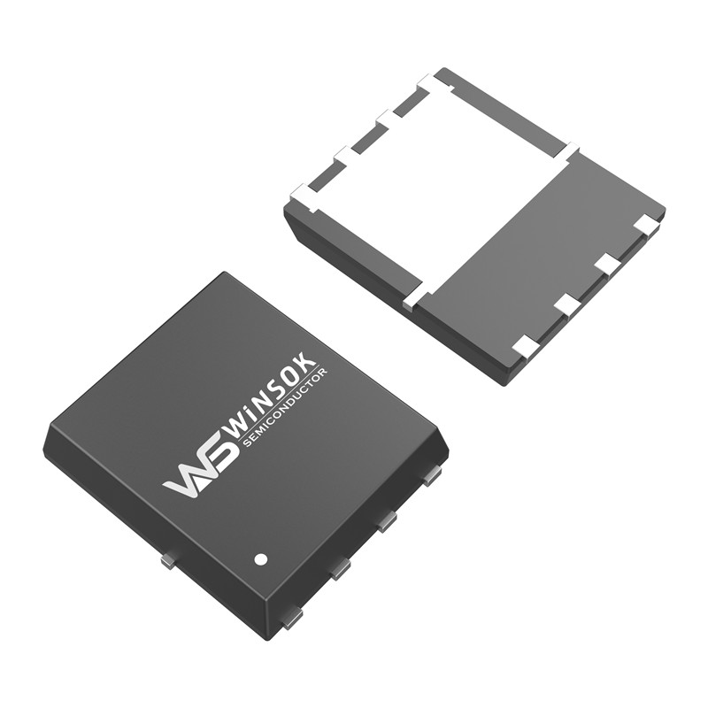
The WSD30140DN56 is the highest performance trench N-channel MOSFET with very high cell density providing excellent RDSON and gate charge for most synchronous buck converter applications. WSD30140DN56 complies with RoHS and green product requirements, 100% EAS guarantee, full function reliability approved.
Advanced high cell density Trench technology.
Ultra-low gate charge with excellent CdV/dt effect attenuation.
100% EAS guarantee, green devices available, RoHS compliant.
Suitable for various high-efficiency power management systems, including:
| Symbol | Parameter | Rating | Units |
|---|---|---|---|
| VDS | Drain-Source Voltage | 30 | V |
| VGS | Gate-Source Voltage | ±20 | V |
| ID@TC=25℃ | Continuous Drain Current, VGS @ 10V1,7 | 85 | A |
| ID@TC=70℃ | Continuous Drain Current, VGS @ 10V1,7 | 65 | A |
| IDM | Pulsed Drain Current2 | 300 | A |
| PD@TC=25℃ | Total Power Dissipation4 | 50 | W |
| TSTG | Storage Temperature Range | -55 to 150 | ℃ |
| TJ | Operating Junction Temperature Range | -55 to 150 | ℃ |
| Symbol | Parameter | Conditions | Min. | Typ. | Max. | Unit |
|---|---|---|---|---|---|---|
| BVDSS | Drain-Source Breakdown Voltage | VGS=0V , ID=250uA | 30 | --- | --- | V |
| △BVDSS/△TJ | BVDSS Temperature Coefficient | Reference to 25℃, ID=1mA | --- | 0.02 | --- | V/℃ |
| RDS(ON) | Static Drain-Source On-Resistance2 | VGS=10V , ID=20A | --- | 1.7 | 2.4 | mΩ |
| VGS=4.5V , ID=15A | --- | 2.5 | 3.3 | |||
| VGS(th) | Gate Threshold Voltage | VGS=VDS , ID =250uA | 1.2 | 1.7 | 2.5 | V |
| IDSS | Drain-Source Leakage Current | VDS=24V , VGS=0V , TJ=25℃ | --- | --- | 1 | uA |
| VDS=24V , VGS=0V , TJ=55℃ | --- | --- | 5 | |||
| IGSS | Gate-Source Leakage Current | VGS=±20V , VDS=0V | --- | --- | ±100 | nA |
| gfs | Forward Transconductance | VDS=5V , ID=20A | --- | 90 | --- | S |
| Qg | Total Gate Charge (4.5V) | VDS=15V , VGS=4.5V , ID=20A | --- | 26 | --- | nC |
| Qgs | Gate-Source Charge | --- | 9.5 | --- | ||
| Qgd | Gate-Drain Charge | --- | 11.4 | --- | ||
| Td(on) | Turn-On Delay Time | VDD=15V , VGEN=10V , RG=3Ω, RL=0.75Ω. | --- | 11 | --- | ns |
| Tr | Rise Time | --- | 6 | --- | ||
| Td(off) | Turn-Off Delay Time | --- | 38.5 | --- | ||
| Tf | Fall Time | --- | 10 | --- | ||
| Ciss | Input Capacitance | VDS=15V , VGS=0V , f=1MHz | --- | 3000 | --- | pF |
| Coss | Output Capacitance | --- | 1280 | --- | ||
| Crss | Reverse Transfer Capacitance | --- | 160 | --- |
It is widely used in high-frequency point-of-load synchronization, buck converters, networked DC-DC power systems, electric tools, electronic cigarettes, wireless charging, drones, medical equipment, car charging, controllers, digital products, and other consumer electronics.
The Drain-Source Breakdown Voltage (BVDSS) is 30V, and it features a continuous drain current (ID) of up to 85A under a gate-source voltage (VGS) of 10V at TC=25℃.
At VGS=10V and ID=20A, the typical RDS(ON) is 1.7mΩ (Max 2.4mΩ). At VGS=4.5V and ID=15A, the typical RDS(ON) is 2.5mΩ (Max 3.3mΩ).
Yes, it is fully compliant with RoHS and green product requirements, features full function reliability approval, and offers a 100% EAS (Energy Avalanche) guarantee.
Equivalent cross-reference parts include Alpha & Omega's AON6312 and AON6358, ON Semiconductor's NTMFS4847N, Vishay's SiRA62DP, STMicroelectronics' STL86N3LLH6AG, and Infineon's BSC050N03MSG, among others.
The operating junction temperature range (TJ) and storage temperature range (TSTG) for this device are from -55 to 150 ℃.