Optimized silicon solutions offering replacement equivalence for tier-1 global brands with guaranteed parametric matching.

HONGKONG Olukey Industry Co., Limited is a premier solution provider focusing on the overall integration of high-performance electronic components. We maintain three distinct, vertically integrated product lines designed to service high-reliability applications: WINSOK MOSFETs, Cmsemicon MCUs, and customized PCBA circuit board development.
At present, Olukey Industry solutions are widely integrated into mission-critical infrastructures, including automotive electronics, defense-grade microelectronics, industrial automation systems, renewable energy systems, digital medical hardware, 5G telecommunication arrays, IoT modules, and smart household technologies. By leveraging global direct agency partnerships with major semiconductor fabricators, we serve the Asia-Pacific region and international manufacturing hubs.
Why global technology firms rely on Olukey Industry for strategic semiconductor sourcing.
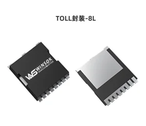
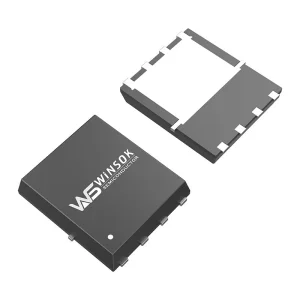
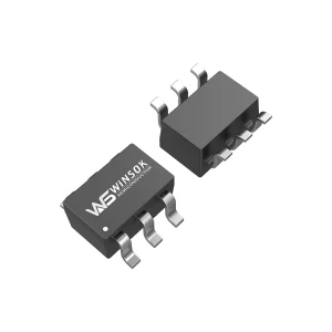
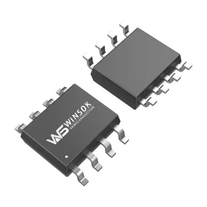
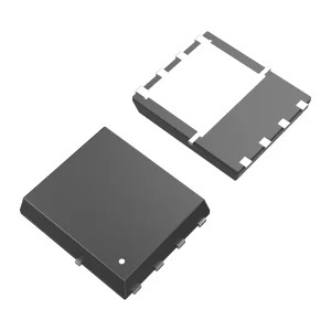
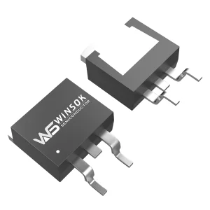
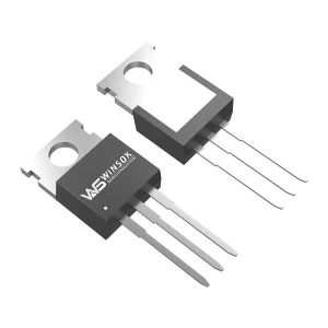
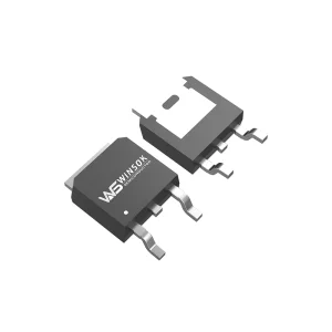
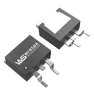
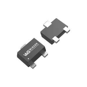
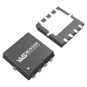
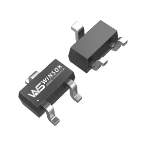
Offering over 600 models across more than 40 standard and custom packages (including DFN3X3-8, DFN5X6-8, TO-252, TO-263, SOP-8, SOT-23, TO-220, and TOLLA-8L) covering the full medium-to-low voltage product spectrum.
Adhering strictly to a "Quality First, Service First" engineering policy. We provide replacement solutions with fast lead times, reducing the supply chain risks associated with tier-1 component shortages.
Our medium and low voltage power MOSFET array spans from 15V, 20V, 30V, 40V, 60V, 80V, 100V, to high-efficiency configurations up to 650V, addressing various power distribution architectures.
Our core mission is to serve as a reliable partner in the global semiconductor sector. We work closely with wafer fabrication plants and package-assembly houses to deliver high-quality components and support market expansion.

Integrating fabrication, testing, and modern packaging technologies to ensure component reliability.




Modern hyperscale data centers, driven by compute-intensive workloads such as Artificial Intelligence (AI) training, machine learning inference, and high-performance computing (HPC), are placing demands on power distribution systems. Legacy 12V intermediate power rails are giving way to 48V distribution schemes. This transition reduces resistive line losses ($I^2R$) by a factor of 16, allowing racks to scale to 100kW and beyond.
However, migrating to a 48V bus requires power semiconductor solutions at the server-board and rack levels. Intermediate Bus Converters (IBC), Voltage Regulator Modules (VRM), and point-of-load (POL) buck converters must achieve conversion efficiencies exceeding 98%. Under these conditions, the selection of power MOSFETs becomes critical. System designers look for alternatives to traditional tier-1 semiconductors that maintain reliability while mitigating cost and supply risks.
China's power semiconductor ecosystem has matured from producing entry-level components to manufacturing high-power, high-frequency devices. Chinese ODM (Original Design Manufacturer) MOSFET factories are now viable alternatives for global companies due to several key factors:
In server hardware design, MOSFETs are used across three main power conversion stages:
Primary-Side Switching in server Power Supply Units (PSUs): Typically operating at 380V DC after Power Factor Correction (PFC), these topologies utilize superjunction or high-voltage planar MOSFETs. Minimizing switching losses ($E_{on}$ and $E_{off}$) and output capacitance energy ($E_{oss}$) in these stages is essential to meet the Climate Savers Computing Initiative's 80 PLUS Titanium efficiency standards.
Secondary-Side Synchronous Rectification: In LLC resonant converters or phase-shifted full-bridge converters, low-voltage, high-current MOSFETs (e.g., 40V, 60V, or 80V in TOLLA or DFN5x6 packages) replace traditional output diodes. Achieving low $R_{DS(on)}$ reduces conduction losses when carrying currents that can exceed 200A.
Point-of-Load (POL) Converters & Smart Power Stages (SPS): Placed next to CPUs, GPUs, and ASICs, these buck converters drop intermediate rails down to core voltages (often sub-1V). MOSFETs in these applications must switch at high frequencies (300kHz to 1.5MHz) to reduce the footprint of inductors and capacitors. These devices require low gate charge ($Q_g$) to minimize gate driver power dissipation.
Geopolitical shifts and supply chain constraints have made dual-sourcing a standard strategy for global procurement teams. Relying on a single supplier for power switches increases risk. Incorporating ODM MOSFETs from Chinese manufacturers like WINSOK into the bill of materials (BOM) provides several strategic advantages:
First, it establishes supply security. If a primary supplier experiences disruptions, production lines can quickly pivot to qualified secondary components. Second, it creates competitive pricing dynamics, helping to control overall BOM costs.
To qualify an alternative component, engineers should follow a structured verification process:
Addressing technical and logistical questions from procurement officers and hardware engineers.
Browse additional low-voltage and medium-voltage alternatives for server motherboards and telecom systems.
 Olukey