In modern Switched-Mode Power Supplies (SMPS), the silicon core dictates performance, conversion efficiency, and thermal limits. For decades, global tier-1 manufacturers dominated key portfolios, exposing developers to high market volatility. The electronics industry now faces constant market disruptions, shifting lead times, and sudden allocations of critical components. For engineers and sourcing directors, finding a premium OEM MOSFET for SMPS alternative is no longer just a backup option—it is a core strategy to protect production runs and ensure profitability.
An effective alternative strategy requires matching more than just physical pinouts. It demands an in-depth understanding of silicon performance parameters like Gate-to-Source Charge ($Q_{gs}$), Gate-to-Drain Charge ($Q_{gd}$), Output Capacitance ($C_{oss}$), and Static Drain-Source On-Resistance ($R_{DS(on)}$). These parameters collectively define the Figure of Merit ($FOM = R_{DS(on)} \times Q_g$). Lowering the FOM directly reduces conduction and switching losses, which improves overall power density in telecommunications, industrial adapters, and consumer chargers.

HONGKONG Olukey INDUSTRY CO., LIMITED is an all-in-one components partner. We focus on three main product lines: WINSOK MOSFET, Cmsemicon MCU, and custom PCBA design. We help manufacturers replace single-sourced components with qualified, cost-effective alternatives.
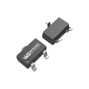
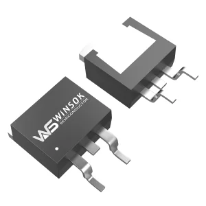
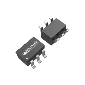
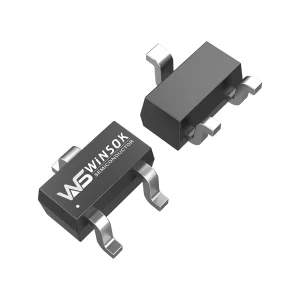
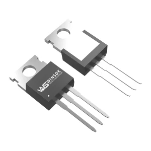
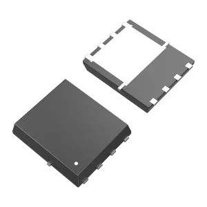
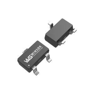
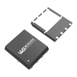
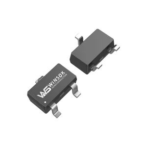
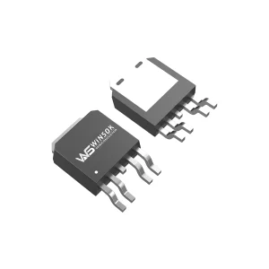
We supply a wide range of low and medium-voltage MOSFETs. Voltage options include: 15V, 20V, 30V, 40V, 60V, 80V, 100V, 120V, 150V, 200V, 250V, 300V, 400V, 500V, 600V, and 650V. We provide pin-compatible drop-in replacements for standard packages including DFN3X3-8, DFN5X6-8, TO-252, TO-263, SOP-8, SOT-23, and TO-220.
Our products feature advanced planar and trench technologies. By offering over 600 models and 40 package types, we provide stable, industry-compliant alternatives that help shield your supply chain from shortages.

Leveraging direct-from-factory logistics in Chinese semiconductor hubs offers significant advantages in cost, lead time, and capacity. The Shenzhen and Hong Kong industrial corridors host a complete ecosystem for wafer processing, advanced packaging, and rigorous testing. This vertical integration allows us to keep large stocks of high-demand MOSFET parts ready for immediate delivery.
We avoid long tier-1 distributor queues by working directly with original factories. This close partnership enables us to offer:
Global OEMs and EMS providers require components that meet strict performance, quality, and regulatory standards. Our products undergo thorough testing to ensure they match or exceed the performance of traditional Tier-1 semiconductor parts.
Each batch is subjected to rigorous testing, including high-temperature reverse bias (HTRB), high-temperature gate bias (HTGB), and pressure cooker tests (PCT). This ensures stable, long-term performance under demanding operating conditions.
All devices are fully compliant with RoHS and REACH standards. We provide lead-free, halogen-free packaging solutions to meet strict global environmental requirements.
Our MOSFETs feature standard footprints (e.g., DFN5X6-8, TO-220, SOT-23) that match industry-standard specifications. This allows drop-in replacement on existing PCBs, eliminating the need for costly board redesigns.




When replacing a MOSFET in high-frequency SMPS applications, engineers must balance thermal limits, gate drive current, and transient voltages. The table below outlines typical parameter ranges for common package types, helping you select the appropriate WINSOK alternative:
| Typical Packaging | Voltage Range (V_DS) | On-Resistance (R_DS(on)) | Gate Charge (Q_g Typ) | Recommended Applications |
|---|---|---|---|---|
| DFN3X3-8 / DFN5X6-8 | 20V - 100V | 1.2mΩ - 8.5mΩ | 15nC - 45nC | Synchronous Rectification, DC-DC Converters, Fast-Chargers |
| TO-252 (DPAK) / TO-263 | 30V - 150V | 2.5mΩ - 18mΩ | 30nC - 80nC | Motor Drives, Main Switching in SMPS, Industrial PSU |
| SOP-8 / SOT-23 | -30V - 60V | 8mΩ - 45mΩ | 5nC - 18nC | Portable devices, LED Backlighting, Low-power Buck regulators |
| TO-220 / TO-220F-3L | 100V - 650V | 0.18Ω - 1.2Ω | 25nC - 75nC | High-voltage Flyback, Server Power Supplies, PFC Stages |
By matching package footprints and critical electrical parameters ($V_{DS}$, $R_{DS(on)}$, and $Q_g$), designers can safely replace hard-to-source components. This maintains system efficiency without requiring modifications to the gate drive circuitry or thermal heat sinks.
High-density USB-C adapters require low switching losses. Our DFN5X6-8 N-channel MOSFETs deliver low gate charge, enabling operating frequencies above 100 kHz while maintaining low operating temperatures.
Modern server power supplies rely on high-efficiency synchronous rectification. Our low-$R_{DS(on)}$ TO-220 and TO-263 devices reduce conduction losses, helping power systems achieve 80-Plus Titanium efficiency ratings.
Industrial environments present regular voltage transients. Our 600V and 650V TO-220F-3L Super-Junction series provide robust avalanche energy ($E_{AS}$) ratings to prevent damage from power line surges.
The power electronics industry is shifting toward higher power density and integration. While Wide Bandgap (WBG) materials like Gallium Nitride (GaN) and Silicon Carbide (SiC) are growing in high-end applications, silicon-based MOSFETs remain the primary choice for standard power supplies due to their cost-efficiency and proven reliability.
Key developmental focuses for silicon MOSFETs include:

 Olukey