Engineered for high thermal efficiency and ultra-low RDS(on), optimizing power density and extending system lifespan.
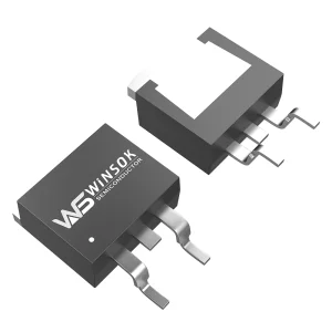
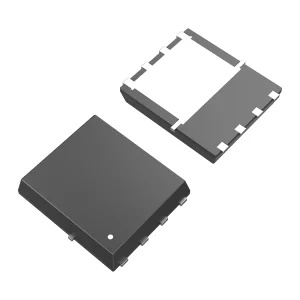

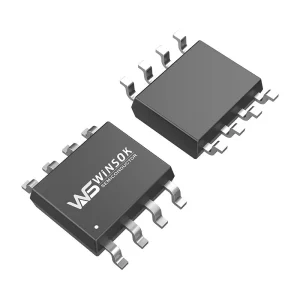
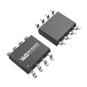
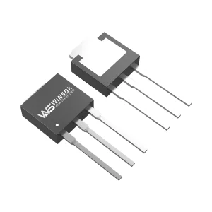
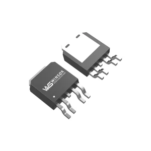
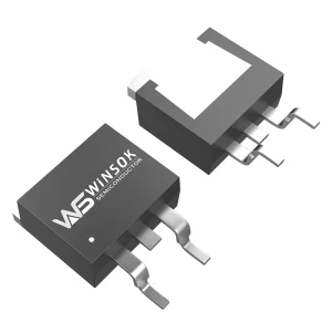
The global transition to electrification has placed lithium-ion battery management systems (BMS) at the center of modern industrial innovation. Power MOSFETs serve as the critical gatekeepers within these circuits, regulating charge and discharge rates, isolating faulty cells, and protecting sensitive systems from overvoltage, undervoltage, and thermal runaway. From micro-mobility solutions like e-bikes to high-voltage industrial Energy Storage Systems (ESS), selecting the correct MOSFET design directly dictates system efficiency, safe operating area (SOA), and overall safety parameters.
In high-capacity Li-ion configurations, transient thermal stability is paramount. Standard planar technologies are increasingly replaced by shielded-gate trench structures that significantly lower the specific on-resistance ($R_{DS(on)}$ per unit area) and minimize total gate charge ($Q_g$). These advancements allow design engineers to boost switching speeds and minimize switching losses, which is vital for preventing local hotspots on the PCB. Hardware engineers prioritize components that boast reliable avalanche ruggedness ($E_{AS}$) and robust package-level thermal impedance ($R_{\theta JC}$), ensuring survivability under short-circuit conditions.
Key Design Constraint: Minimizing power dissipation in multi-cell packs is not just about battery life; it is a critical safety parameter to prevent thermal cascading within compact battery enclosures.
Original Equipment Manufacturers (OEMs) face persistent supply chain friction, lead-time uncertainty, and end-of-life (EOL) announcements from legacy semiconductor suppliers. Sourcing a dependable second-source or cross-reference counterpart for popular part numbers is essential for maintaining production continuity. However, cross-referencing power MOSFETs is not simply about matching footprint dimensions. A thorough validation process must cross-reference dynamic parameters, package dissipation ratings, body diode recovery characteristics ($t_{rr}, Q_{rr}$), and gate-source threshold voltages ($V_{GS(th)}$). A discrepancy in these values can cause parasitic oscillations, excessive heat generation, or premature driver circuit failure.
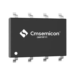
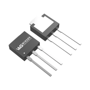
HONGKONG Olukey INDUSTRY CO., LIMITED operates as a premium solution provider specializing in the full-scale development, testing, and distribution of electronic component solutions. Our portfolio spans three core divisions: high-reliability WINSOK MOSFETs, Cmsemicon MCUs, and custom PCBA circuit board solutions designed to streamline system integration.
By positioning our operation at the center of the Asia-Pacific supply chain and leveraging global general agency access to original semiconductor fabs, we bridge the gap between premium silicon design and cost-effective manufacturing. We don't just supply parts; we provide deep technical support to assist design teams in executing drop-in cross-reference qualifications without sacrificing board-level efficiency or safety margins.
Our Core Promise: Complete parametric compatibility testing, comprehensive FAE review of schematics, and secure inventory reservation models to eliminate sourcing disruptions.

Our multi-channel validation protocols guarantee that cross-referenced devices perform reliably under harsh electrical conditions.
Our solutions range across more than 40 package styles, including high-power density DFN3X3-8, DFN5X6-8, SOP-8, robust TO-252, TO-263, and compact SOT-23, covering over 600 unique models.
From ultra-low voltage battery protectors to high-voltage industrial converters, our portfolio covers 15V, 20V, 30V, 40V, 60V, 80V, 100V, 120V, 150V, 200V, 250V, 300V, 400V, 500V, 600V, and 650V.
We maintain strict ISO 9001 quality management across all production lines. Each batch undergoes 100% dynamic testing and avalanche energy screening to ensure zero-defect shipment standards.

China's semiconductor cluster provides unmatched speed, flexibility, and cost efficiency. Operating from the heart of Shenzhen and global logistics networks, our manufacturing lines integrate high-throughput front-end wafer fabrication with advanced packaging and testing facilities. This geographic consolidation cuts lead times from weeks to days, allowing quick production adjustments that Western fabs cannot match.
Our automated die-attach, wire-bonding, and high-density packaging lines optimize silicon yield and thermal efficiency. By using standard footprints like DFN5x6 and TO-220, we can easily match specifications for major global brands like Infineon, Onsemi, Vishay, and AOS, helping customers easily manage global supply chain risks.
A visual look into our high-speed surface mount assembly lines, cleanrooms, and testing facilities.





Power MOSFET requirements vary significantly across different battery-powered industries. To help design engineers choose the right cross-reference parts, we analyze four major application scenarios below.
E-mobility systems require low switching losses and excellent thermal handling under continuous peak loads. During acceleration, currents can spike up to 5-10 times the normal operating rate. MOSFETs in these systems, typically in TO-263, TO-220, or DFN5x6-8 packages, must have high avalanche energy ratings ($E_{AS}$) to absorb back-EMF spikes from the motor during regenerative braking.
In smart wearables and smartphones, space is the primary design constraint. Engineers prioritize ultra-compact footprints like DFN2X2-6, DFN3X3-8, and chip-scale packages. These applications run at lower currents, making low gate threshold voltages ($V_{GS(th)}$ down to 0.5V to 1.5V) critical, enabling direct operation from low-voltage microcontroller I/O pins without dedicated gate drivers.
Power tools run at high power levels in short, intense bursts, creating heavy thermal stress. Power MOSFETs must deliver low $R_{DS(on)}$ (often under 1.5mΩ) to prevent rapid temperature buildup. Our DFN5x6 and TO-252 packages utilize advanced copper clip bonding rather than thin aluminum wire bonds, dramatically lowering parasitic package resistance and boosting current-carrying capacity.
Industrial backup systems run at higher voltages (48V to 400V+), demanding MOSFET ratings of 80V, 100V, 150V, or higher. In these multi-cell topologies, safe operating area (SOA) margin and low drain-to-source leakage currents ($I_{DSS}$) are critical for preventing cell self-discharge during long standby periods.
A reference guide showing how WINSOK MOSFETs match industry-standard packages and ratings.
| WINSOK Series | Package Style | Voltage ($V_{DSS}$) | On-Resistance ($R_{DS(on)}$ Max) | Typical Equivalent Competitor Lines | Target Applications |
|---|---|---|---|---|---|
| WSD30160DN56 | DFN5X6-8L | 30V | 1.4 mΩ @ 10V | Infineon BSC014N03SG, ON Semi FDMS7602S, AOS AON6512 | E-Bike BMS, High-Current Switchers |
| WSK140N03 | TO-263-2L | 30V | 2.1 mΩ @ 10V | Vishay SUM110N03, Infineon IPB023N03L, Fairchild FDB8896 | Power Tools, Battery Protection Switches |
| WSP4016 | SOP-8L | 40V | 6.5 mΩ @ 10V | AOS AO4407A, Vishay Si4484EY, Diodes Inc DMN4026SSD | Smart Battery Packs, Multi-Cell Charger Protection |
| WSF160N10 | TO-252-2L | 100V | 5.8 mΩ @ 10V | Onsemi FDD86102, Infineon IPD060N10N3G, Vishay SUD50N10 | Industrial ESS, Telecom Battery Banks, Solar BMS |
| WST2035 | TO-263-2L (P-Ch) | -20V | 12.0 mΩ @ -4.5V | Vishay SUB75P03-07, AOS AOB411, Onsemi FDB4436 | Load Switch, High-Side Battery Disconnect Circuits |
The power semiconductor landscape is evolving rapidly to meet the needs of next-generation green energy systems. As lithium iron phosphate ($LiFePO_4$) and solid-state battery configurations grow in popularity, system voltages are rising. This shifts demand toward 100V-150V MOSFETs with extremely low gate charge ($Q_{gd}$) to prevent self-turn-on in high $dV/dt$ environments.
Packaging technology is also shifting away from wire-bonded designs like TO-220 to surface-mount packages such as DFN5x6-8, DFN3x3-8, and LFPAK. These packages reduce parasitic source inductance, helping prevent voltage ringing during fast turn-off cycles. Lead-less packages also enable top-side cooling, allowing designers to attach thermal interface materials directly to external heatsinks. This improves thermal performance and helps reduce overall board size.
Additionally, microcontrollers are increasingly integrated with analog front-ends (AFE) and driver stages on a single board, as seen in Cmsemicon MCU developments. This high-density integration requires power switches to have low gate drive requirements. Logic-level MOSFETs that run efficiently at $V_{GS}$ gate drives of 4.5V or even 2.5V are becoming the industry standard, helping simplify gate driver circuitry and reduce overall component count.
Answers to common questions from design engineers and procurement teams on selecting and validating power MOSFETs.
High-reliability components designed to meet strict industrial and consumer electronic standards.


 Olukey