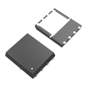
Latest design WSD30160DN56 N-channel 30V 120A DFN5X6-8 WINSOK MOSFET Factories, Distributors

Part Number:WSD30160DN56 BVDSS:30V ID:120A RDSON:1.9mΩ   Channel:N-channel Package:DFN5X6-8

Product Description

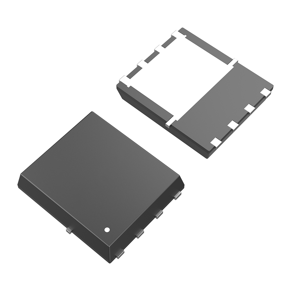
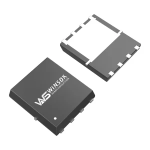
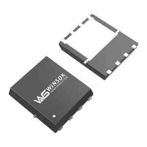
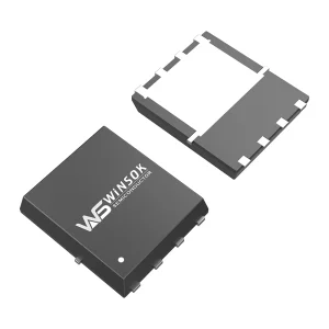
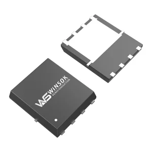
WSD30160DN56 N-Channel MOSFET The WSD30160DN56 MOSFET operates at a voltage of 30V with a current capacity of 120A and a low resistance of 1.9mΩ. Designed as an N-channel MOSFET, it is housed in a high-thermal-efficiency DFN5X6-8 package.
Voltage 30V
Current 120A
Resistance 1.9mΩ
Package DFN5X6-8

Target Applications

E-cigarettes Wireless Charging Drones Medical Care Car Chargers Controllers Digital Products Small Household Appliances Consumer Electronics

Cross Reference & Replacement Models

AOS MOSFET AON6382, AON6384, AON644A, AON6548
Onsemi / Fairchild MOSFET NTMFS4834N, NTMFS4C5N
Toshiba MOSFET TPH2R93PL
Panjit MOSFET PJQ5426
Niko-Sem MOSFET PKE1BB
Potens Semiconductor MOSFET PDC392X

Absolute Maximum Ratings

Symbol Parameter Rating Units
VDS Drain-Source Voltage 30 V
VGS Gate-Source Voltage ±20 V
ID @ TC=25℃ Continuous Drain Current, VGS @ 10V1,7 120 A
ID @ TC=100℃ Continuous Drain Current, VGS @ 10V1,7 68 A
IDM Pulsed Drain Current2 300 A
EAS Single Pulse Avalanche Energy3 128 mJ
IAS Avalanche Current 50 A
PD @ TC=25℃ Total Power Dissipation4 62.5 W
TSTG Storage Temperature Range -55 to 150
TJ Operating Junction Temperature Range -55 to 150

Electrical Characteristics (TJ=25℃ unless otherwise noted)

Symbol Parameter Conditions Min. Typ. Max. Unit
BVDSS Drain-Source Breakdown Voltage VGS=0V, ID=250uA 30 --- --- V
△BVDSS/△TJ BVDSS Temperature Coefficient Reference to 25℃, ID=1mA --- 0.02 --- V/℃
RDS(ON) Static Drain-Source On-Resistance2 VGS=10V, ID=20A --- 1.9 2.5
VGS=4.5V, ID=15A --- 2.9 3.5
VGS(th) Gate Threshold Voltage VGS=VDS, ID=250uA 1.2 1.7 2.5 V
△VGS(th) VGS(th) Temperature Coefficient --- -6.1 --- mV/℃
IDSS Drain-Source Leakage Current VDS=24V, VGS=0V, TJ=25℃ --- --- 1 uA
VDS=24V, VGS=0V, TJ=55℃ --- --- 5
IGSS Gate-Source Leakage Current VGS=±20V, VDS=0V --- --- ±100 nA
gfs Forward Transconductance VDS=5V, ID=10A --- 32 --- S
Rg Gate Resistance VDS=0V, VGS=0V, f=1MHz --- 0.8 1.5 Ω
Qg Total Gate Charge (4.5V) VDS=15V, VGS=4.5V, ID=20A --- 38 --- nC
Qgs Gate-Source Charge --- 10 ---
Qgd Gate-Drain Charge --- 13 ---
Td(on) Turn-On Delay Time VDD=15V, VGEN=10V, RG=6Ω, ID=1A, RL=15Ω --- 25 --- ns
Tr Rise Time --- 23 ---
Td(off) Turn-Off Delay Time --- 95 ---
Tf Fall Time --- 40 ---
Ciss Input Capacitance VDS=15V, VGS=0V, f=1MHz --- 4900 --- pF
Coss Output Capacitance --- 1180 ---
Crss Reverse Transfer Capacitance --- 530 ---

Frequently Asked Questions

What are the core electrical ratings of the WSD30160DN56 MOSFET?
The WSD30160DN56 is an N-channel MOSFET designed for a maximum Drain-Source voltage (VDS) of 30V, a continuous current (ID) of 120A at 25℃, and exhibits a highly efficient typical on-resistance (RDS(ON)) of 1.9mΩ at a gate drive of 10V.
In what applications is the WSD30160DN56 typically used?
Thanks to its high current threshold and low internal resistance, it is widely integrated into e-cigarettes, wireless charging stations, drones, medical equipment, car chargers, smart controllers, small household appliances, and various digital consumer electronics.
What package type does the WSD30160DN56 use?
This MOSFET uses a DFN5X6-8 surface-mount package. The compact, flat-lead design offers excellent thermal dissipation and layout performance in high-density electronic circuits.
Are there suitable cross-reference replacement models from other manufacturers?
Yes, functional equivalents include AOS (AON6382, AON6384, AON644A, AON6548), Onsemi/Fairchild (NTMFS4834N, NTMFS4C5N), Toshiba (TPH2R93PL), Panjit (PJQ5426), Niko-Sem (PKE1BB), and Potens (PDC392X).
What is the gate threshold voltage (VGS(th)) range for this device?
The gate threshold voltage ranges from a minimum of 1.2V up to a maximum of 2.5V, with a typical value of 1.7V, making it highly compatible with standard logic-level drive signals.

Related Products