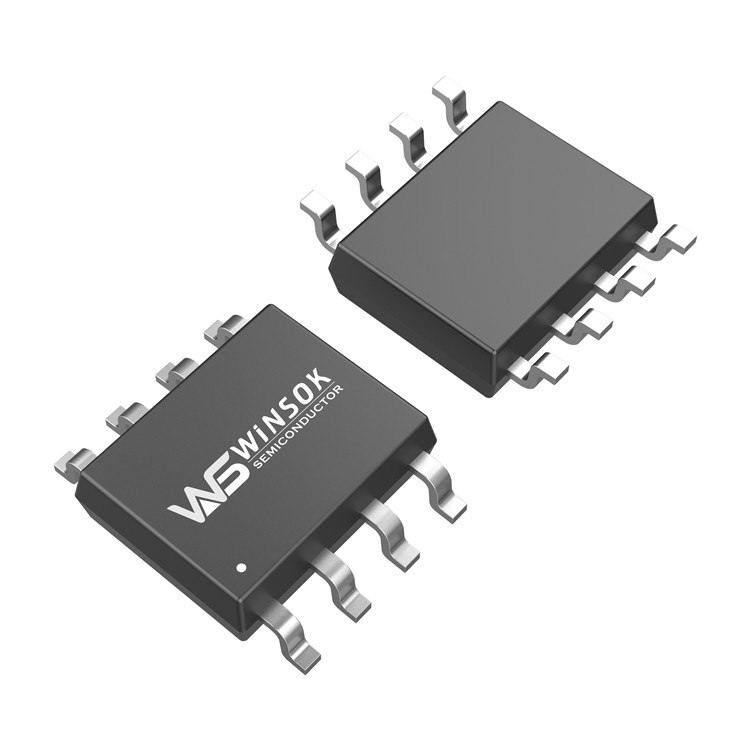
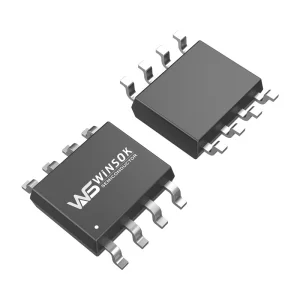
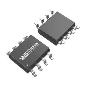
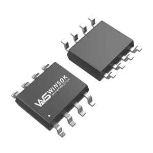
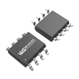
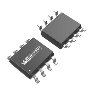
The WSP4016 is the highest performance trench N-ch MOSFET with extreme high cell density, which provides excellent RDSON and gate charges for most of the synchronous buck converter applications. The WSP4016 meets the RoHS and Green Product requirement, 100% EAS guaranteed with full function reliability approved.
Advanced High Cell Density Trench Technology
Super Low Gate Charge
Excellent CdV/dt Effect Decline
100% EAS Guaranteed
Green Device Available
Cross References / Equivalent Models
AO AOSP66406
ON FDS8842NZ
VISHAY Si4840BDY
PANJIT PJL9420
Sinopower SM4037NHK
NIKO PV608BA
DINTEK DTM5420
Absolute Maximum Ratings
Symbol
Parameter
Rating
Units
VDS
Drain-Source Voltage
40
V
VGS
Gate-Source Voltage
±20
V
ID@TC=25℃
Continuous Drain Current, VGS @ 10V1
15.5
A
ID@TC=70℃
Continuous Drain Current, VGS @ 10V1
8.4
A
IDM
Pulsed Drain Current2
30
A
PD@TA=25℃
Total Power Dissipation TA=25°C
2.08
W
PD@TA=70℃
Total Power Dissipation TA=70°C
1.3
W
TSTG
Storage Temperature Range
-55 to 150
℃
TJ
Operating Junction Temperature Range
-55 to 150
℃
Electrical Characteristics
Symbol
Parameter
Conditions
Min.
Typ.
Max.
Unit
BVDSS
Drain-Source Breakdown Voltage
VGS=0V , ID=250uA
40
---
---
V
RDS(ON)
Static Drain-Source On-Resistance2
VGS=10V , ID=7A
---
8.5
11.5
mΩ
VGS=4.5V , ID=5A
---
11
14.5
VGS(th)
Gate Threshold Voltage
VGS=VDS , ID =250uA
1.0
1.8
2.5
V
IDSS
Drain-Source Leakage Current
VDS=32V , VGS=0V , TJ=25℃
---
---
1
uA
VDS=32V , VGS=0V , TJ=55℃
---
---
25
IGSS
Gate-Source Leakage Current
VGS=±20V , VDS=0V
---
---
±100
nA
gfs
Forward Transconductance
VDS=5V , ID=15A
---
31
---
S
Qg
Total Gate Charge (4.5V)
VDS=20V ,VGS=10V ,ID=7A
---
20
30
nC
Qgs
Gate-Source Charge
---
3.9
---
Qgd
Gate-Drain Charge
---
3
---
Td(on)
Turn-On Delay Time
VDD=20V,VGEN=10V,RG=1Ω, ID=1A, RL=20Ω.
---
12.6
---
ns
Tr
Rise Time
---
10
---
Td(off)
Turn-Off Delay Time
---
23.6
---
Tf
Fall Time
---
6
---
Ciss
Input Capacitance
VDS=20V , VGS=0V , f=1MHz
---
1125
---
pF
Coss
Output Capacitance
---
132
---
Crss
Reverse Transfer Capacitance
---
70
---
Applications
White LED boost converters
Automotive Systems
Industrial DC/DC Conversion Circuits
EAutomotive electronics
LED lights & audio
Digital products
Small household appliances
Consumer electronics
Protection boards
Note :
1. Pulse test: PW <= 300us duty cycle <= 2%.
2. Guaranteed by design, not subject to production testing.
Frequently Asked Questions (FAQ)
Q1: What are the key features of the WSP4016 N-ch MOSFET?
A1: The WSP4016 features advanced high cell density Trench technology, super low gate charge, excellent CdV/dt effect decline, and is 100% EAS guaranteed. It is also a certified Green Device meeting RoHS standards.
Q2: What is the maximum Drain-Source Voltage (VDS) and Gate-Source Voltage (VGS) for the WSP4016?
A2: The WSP4016 supports a maximum Drain-Source Voltage (VDS) of 40V and a Gate-Source Voltage (VGS) of ±20V.
Q3: What are the compatible cross-reference models for the WSP4016?
A3: Equivalent and cross-reference models include AO AOSP66406, ON FDS8842NZ, VISHAY Si4840BDY, PANJIT PJL9420, Sinopower SM4037NHK, NIKO PV608BA, and DINTEK DTM5420.
Q4: What is the typical Static Drain-Source On-Resistance (RDS(ON)) of this MOSFET?
A4: The typical RDS(ON) is 8.5 mΩ when VGS is 10V (at ID=7A), and 11 mΩ when VGS is 4.5V (at ID=5A).
Q5: In what applications is the WSP4016 MOSFET typically used?
A5: It is widely used in synchronous buck converters, white LED boost converters, automotive systems, industrial DC/DC conversion circuits, consumer electronics, protection boards, and digital products.
Q6: What is the operating junction temperature range of the WSP4016?
A6: The WSP4016 has a safe operating and storage junction temperature range of -55 to 150 ℃.
 Olukey