Immediate localized inventory of highly stable and low gate charge transistors ready for integration in precision aerospace systems, EV controllers, and switching power adapters.
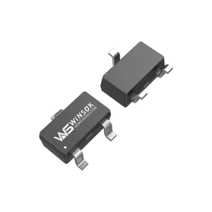
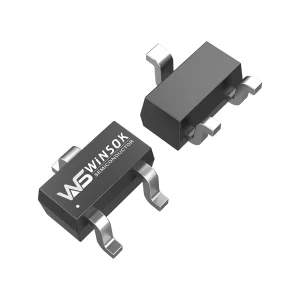

As a global semiconductor powerhouse, Singapore commands over 10% of the world’s microchip manufacturing capability and roughly 20% of the global semiconductor equipment sector. Moving beyond standard assembly, Singapore’s industrial map is transitioning toward high-density power applications, advanced Internet of Things (IoT) ecosystems, and clean green infrastructures as outlined in the Singapore Green Plan 2030.
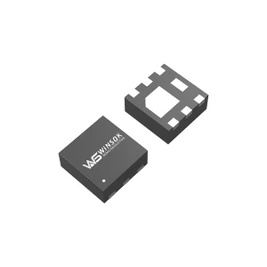
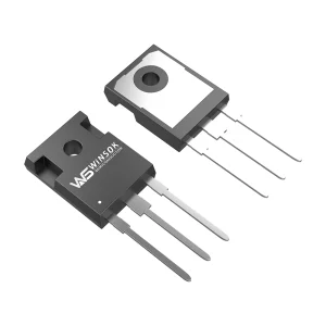
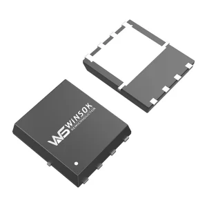
Power management circuits form the backbone of this evolution. Within this context, traditional leaded packages like TO-220 and D2PAK are rapidly giving way to DFN (Dual Flat No-Lead) packages. The transition is driven by space restrictions and thermal performance requirements. DFN3x3 and DFN5x6 devices offer a tiny package footprint while maintaining high current capacity, minimizing parasitic inductance, and enabling low drain-to-source on-resistance ($R_{DS(ON)}$). They are essential component designs in modern, high-frequency, space-constrained power converter architectures.
The electrical and thermal characteristics of DFN packaged MOSFETs differ from traditional package structures in several key ways:
| Package Type | Footprint Area (mm²) | Typical Height (mm) | Thermal Resistance ($R_{\theta JC}$ °C/W) | Parasitic Inductance (nH) |
|---|---|---|---|---|
| TO-220 (Leaded) | ~150.0 | ~4.50 | ~0.5 - 1.5 | ~6.0 - 8.0 |
| TO-252 (DPAK) | ~66.0 | ~2.30 | ~1.0 - 2.5 | ~3.0 - 4.5 |
| DFN 5x6-8L | 30.0 | 0.90 | ~0.8 - 1.8 | ~0.5 - 1.2 |
| DFN 3x3-8L | 9.0 | 0.80 | ~1.5 - 3.0 | ~0.3 - 0.8 |
In Singapore's high-tech zones, including the Jurong Innovation District, Tampines Wafer Fab Parks, and Woodlands, hardware engineers require components with strict parameters and reliable supply lines. Local R&D labs require components that can withstand high humidity and tropical ambient temperatures without thermal failure.
Helping local and international OEM/ODM manufacturers design next-generation electronics with highly integrated semiconductor products.
Singapore hosts over 60% of Southeast Asia’s data center capacity. Power efficiency at the server motherboard level is a critical metric. Using advanced DFN5X6-8L and DFN3X3-8L N-channel MOSFETs in synchronous rectification stages drastically reduces conduction losses. The ultra-low gate-to-drain charge ($Q_{gd}$) enables switching frequencies above 500 kHz, allowing the size of magnetic components to be scaled down for thin rack-mounted server blades.
Under the Land Transport Authority’s initiatives, Singapore is rapidly building out public charging networks. MOSFETs used in onboard chargers (OBC) and DC-DC converters must handle transient surges and high-voltage stress. Winsok's TO-263, TO-252, and high-performance DFN packages supply the power stages with robust drain-source breakdown voltages up to 650V. These devices are designed to run cool and maintain high efficiency in high-ambient environments.
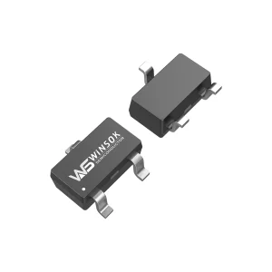
Singapore’s leadership in IoT devices and smart wearable medical systems demands minimal standby drain. Small-footprint MOSFETs like SOT-23-3L, SOT-523-3L, and DFN2X2-6L (e.g., WSD1216DN22) are ideal for battery protection circuits. With low gate threshold voltages ($V_{GS(th)}$), these devices can be driven directly by microcontroller I/O pins, saving PCB space and eliminating the need for external level shifters.




HONGKONG Olukey INDUSTRY CO., LIMITED serves as an integrated solution provider specializing in advanced electronics supply and development. Our portfolio is structured around three core pillars: WINSOK MOSFETs, Cmsemicon MCUs, and comprehensive PCBA design solutions.
By leveraging our network of factory relationships and regional warehouses, we serve the Asia-Pacific region with a direct presence in key industrial centers. We maintain a local buffer stock of critical parts in close proximity to Singapore, providing short lead times and stable pricing to help you manage market fluctuations.
Each batch is tracked via direct factory-original packaging. We provide full certificate of conformance (CoC) documents upon request and ensure compliance with REACH, RoHS, and international IEC safety parameters.
We combine high-performance silicon alternatives with technical support to streamline your design cycle.
The roadmap of MOSFET technology moves toward higher efficiency and integration. Here is what is on the horizon for DFN package architectures:
Newer production runs employ Shielded Gate Trench architectures, which significantly lower $R_{DS(ON)} \times Q_g$ Figure of Merit (FOM). This allows for higher power densities in DFN3.3x3.3 and DFN2x2 packages.
Future thermal solutions will increasingly adopt top-side cooled DFN packages. By allowing heat to flow directly into an attached heatsink from the top of the component, designers can avoid dumping heat into the multi-layer system board, reducing overall board operating temperatures.
While Silicon MOSFETs continue to offer cost-performance advantages, package developments will align with standard footprint structures, allowing drop-in upgrades to wide bandgap modules as system requirements evolve.
Read about packaging, thermal considerations, and cross-compatibility for your designs.
Explore our full catalog of MOSFETs, available in standard packages like DFN, TO-252, TO-263, and SOT. Select a model to learn more or request a quote.

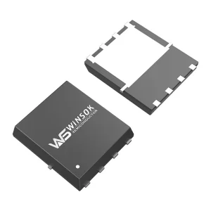
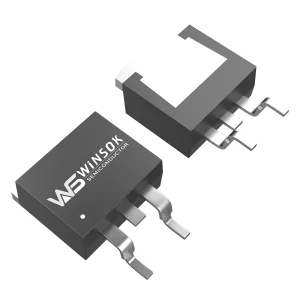
Whether you require engineering samples for a new design or are looking to secure volume production stock, our team is ready to support you with direct technical expertise and reliable logistics.
Send Inquiry Now Olukey