
China MOSFET for BMS Replacement: Design, Sourcing & Reliability

Global Direct Cross-Referencing Guide & Technical Whitepaper for Industrial and Automotive Battery Management Systems

Deep-Dive Whitepaper: Engineering High-Reliability BMS MOSFET Replacements

In the design of modern Battery Management Systems (BMS), the Power MOSFET functions as the primary safety gatekeeper, controlling both charge and discharge currents. With the rapid expansion of electric vehicles (EVs), light electric vehicles (LEVs), energy storage systems (ESS), and portable consumer electronics, the demands placed on these devices have reached unprecedented heights. Selecting a China MOSFET for BMS replacement requires a rigorous understanding of device parameters, physical structures, and material transitions. Engineers must look beyond simple voltage and current ratings to evaluate gate charge ($Q_g$), Safe Operating Area (SOA), and transient thermal impedances.

Historically, global procurement chains relied almost exclusively on tier-1 Western manufacturers. However, systemic supply vulnerabilities and the rapid maturation of Chinese semiconductor fabrication processes have shifted the paradigm. Leading design houses and integrated device manufacturers (IDMs) in China now supply cost-efficient, high-performance MOSFET variants that offer drop-in compatibility and equivalent or superior thermal footprints.

1. Technical Roadmap & Future Outlook

The technological trajectory of BMS MOSFETs is defined by the relentless pursuit of lower specific on-state resistance ($R_{DS(on)} \cdot A$) and improved ruggedness under transient fault conditions. Standard Planar topology has largely given way to Trench architectures, which in turn are being superseded by Split-Gate Trench (SGT) structures.

SGT technology represents a massive leap forward for high-current BMS platforms. By utilizing a shielded gate structure, SGT reduces the gate-to-drain charge ($Q_{gd}$) and the overall gate charge ($Q_g$). This allows design engineers to significantly minimize switching losses while simultaneously squeezing down the $R_{DS(on)}$ per unit area. Looking toward the future, we observe the following trends:

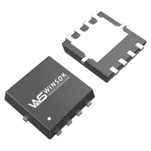
  • Trench vs. SGT Architecture: SGT MOSFETs reduce high-frequency gate ringing and enable much higher power densities in compact packaging like DFN5X6-8L and DFN3X3-8L.
  • Wide-Bandgap Integration: While Silicon (Si) remains the dominant material due to cost-efficiency and mature fabrication techniques, Gallium Nitride (GaN) and Silicon Carbide (SiC) are beginning to see adoption in high-voltage (>400V) ESS and electric drivetrain systems where charging times and thermal dissipation are extremely constrained.
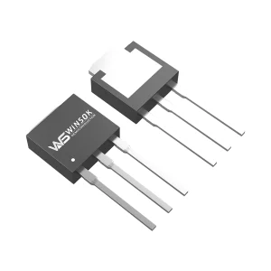
  • Package Evolution: Traditional packages like TO-220 and TO-251 are yielding ground to surface-mount devices (SMDs) featuring bottom-side copper cooling blocks (such as DFN packages). Top-side cooling package options are also emerging to facilitate advanced thermal management strategies where the PCB is no longer the primary heat sink.

2. Macro-Industry Solutions & Device Selection

Different industries demand highly customized BMS topologies. The selection criteria for replacing a MOSFET vary based on cell chemistry ($LiFePO_4$, Li-Ion, LTO) and total stack voltage:

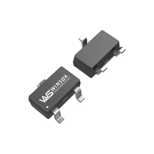
  • Low-Voltage Consumer Pack (1S - 4S): Found in smartphones, power banks, and wearables. These designs require ultra-low gate threshold voltages ($V_{GS(th)}$) to allow full turn-on directly from the microcontroller or analog front-end (AFE) without dedicated gate drivers. Dual N-channel or P-channel configurations in ultra-thin profiles (e.g., SOT-23-3L, DFN3X3-8L) are typical.
  • Medium-Voltage Power Tools & LEVs (5S - 13S): Applications like e-bikes, garden tools, and warehouse automation. These packs encounter highly inductive motor loads, necessitating MOSFETs with excellent avalanche energy ($E_{AS}$) ratings and robust Safe Operating Areas (SOA) to handle the back-EMF during braking or rotor stall conditions.
  • High-Voltage ESS & Industrial Packs (16S - 100S+): Grid storage, solar backups, and telecom power. Systems require series-connected arrays of MOSFETs or massive parallel structures. Devices must possess tight parameter matching (particularly $V_{GS(th)}$ and $R_{DS(on)}$ temperature coefficients) to prevent current hogging and localized thermal runaway. Common voltages for these cells range from 80V to 150V.


Industry 4.0 Standard

China's modernized silicon fabs operate with fully automated process controls, ensuring PPM level defect rates matching global benchmarks.

Drop-In Equivalence

Direct replacements for common footprints (DFN, TO, SOP, SOT) with optimized parasitic parameters for easier PCB cross-referencing.

Supply Chain Security

Mitigate lead-time uncertainties. With localized raw material access and domestic packaging, lead times are compressed by up to 60% compared to traditional channels.

Direct Equivalent Cross-Referencing Guide

The table below details typical parameter targets for replacing legacy Western devices with advanced Chinese equivalents, maintaining optimal margins for system safety.

Typical Part Class BMS Application Type Key Target Parameters China Replacement Package Target Replacement Focus
30V N-Channel (Dual) 1S-2S Smart Devices Vds=30V, Rds(on) < 20mΩ DFN3X3-8L / SOP-8L Maximize efficiency, minimize space
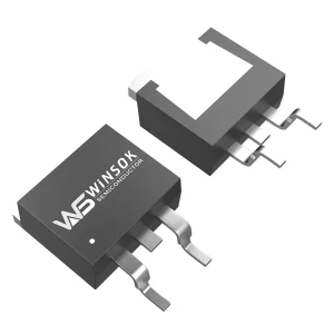
60V-80V N-Channel 10S-13S E-Bikes & Tools Vds=60V-80V, Id=60A-140A TO-252 / TO-263-2L High avalanche ruggedness ($E_{AS}$), thermal stability
100V-150V SGT N-Channel 16S LiFePO4 ESS & Telecom Vds=100V-150V, Id > 100A DFN5X6-8L / TO-263 / TO-220 Low Qg, high power density, thermal cycling life
-20V to -60V P-Channel High-Side Charging Switch Vds=-20V to -60V SOT-23-3L / DFN5X6-8L Eliminate charge pump gate drive requirements
< 1.5 mΩ
Ultra-Low Rds(on)
600+
Production Models
40+
Package Styles
100%
AQL Tested & Approved

3. China Factory 4.0: Supply Chain Resilience & Efficiency Advantages

The modern Chinese semiconductor manufacturing landscape is built upon a foundation of highly integrated industrial clusters and advanced automation. Leveraging vertical integration, design firms and packaging foundries collaborate closely to optimize the feedback loop between physical design and wafer yield.

By utilizing state-of-the-art 8-inch and 12-inch wafer processing facilities, factories achieve exceptional consistency in channel doping, gate oxide thickness, and trench depth. This automation directly translates to a tighter distribution of electrical parameters (such as $V_{GS(th)}$ and leakage currents), which is crucial for systems that use parallel MOSFET groups. A tight parameter tolerance minimizes unbalanced current loads, ensuring no single device is subjected to excess stress during high-rate charging or short-circuit events.

Furthermore, domestic packaging ecosystems reduce global logistics latency. Rather than routing chips through multiple regional packaging, testing, and distribution centers, our integrated network conducts fabrication, assembly, and reliability validation within unified industrial zones. This streamlined logistics infrastructure ensures stable lead times and protects global buyers from sudden macroeconomic shocks.

4. Sourcing Requirements for Global Enterprises

For global engineering and procurement departments, replacing a semiconductor component is not simply a matter of swapping out part numbers. It requires satisfying rigorous quality assurance standards, logistical validation, and regulatory compliance. The key requirements include:

  • E-E-A-T and Quality Assurance: The replacement manufacturer must provide complete documentation, including material composition datasheets, reliability reports (covering High-Temperature Gate Bias (HTGB), High-Temperature Reverse Bias (HTRB), and Temperature Cycling (TC)), and trace history back to the wafer lot.
  • Regulatory Standards: All components must comply with RoHS and REACH directives, ensuring the absence of hazardous substances. Certifications must be kept current and verified by independent testing laboratories.
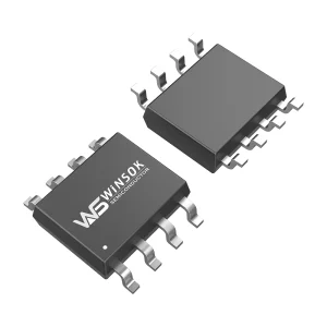
  • Form-Fit-Function Drop-In Testing: Evaluation begins with cross-referencing package footprints (e.g., matching a competitor's SO-8 or DFN5x6 to the corresponding local part number). Next, gate drive compatibility must be validated to ensure the existing gate drivers do not overheat or exhibit slow switching times. Finally, dynamic testing under peak load and short-circuit conditions is required to verify the safety margins of the replacement device.
Hongkong Olukey Industry Facilities

Corporate Profile: Hongkong Olukey Industry Co., Limited

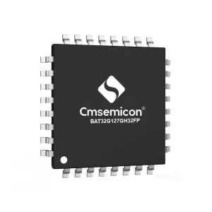
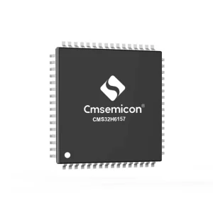
HONGKONG Olukey INDUSTRY CO., LIMITED is a comprehensive solution provider focusing on the overall integration of high-performance electronic components. The core business lines comprise three primary technological vectors: WINSOK MOSFETs, Cmsemicon MCUs, and customized PCBA circuit board solution development.

At present, Olukey Industry solutions are widely adopted in automotive electronics, military systems, smart industrial controls, new energy ecosystems, advanced medical devices, 5G infrastructure, IoT terminals, smart home appliances, and consumer electronics. Leveraging the supply channels of major original component factories, Olukey provides advanced high-tech electronic components and professional application support to developers and manufacturers worldwide.

Why Choose Us

We provide comprehensive, high-quality technical support and logistical services to supply customers with advanced electronic components. By adhering to the principles of "quality first, service first," Olukey has established long-term cooperative partnerships with high-tech enterprises and manufacturers worldwide, securing reputation through sustained component reliability.

WINSOK Voltage Capabilities

WINSOK MOSFET's product line spans medium and low voltages: 15V, 20V, 30V, 40V, 60V, 80V, 100V, 120V, 150V, 200V, 250V, 300V, 400V, 500V, 600V, and 650V. We provide more than 600 models across 40 distinct package form factors to satisfy a wide range of industrial and consumer power topologies.

Complete Integrated Solutions

By pairing Cmsemicon MCU design capabilities with WINSOK MOSFETs, Olukey provides a unified development platform for battery management, motor control, and smart home appliances. We work closely with engineers from initial prototyping through to final PCBA assembly.

Automated Testing Line
Surface Mount SMT Process
Component Warehouse Quality Control

Expanding Global Technical Support

Semiconductor sourcing demands high-quality localized support to handle technical issues, field failures, and regulatory requests. Olukey maintains engineering support nodes and localized distributor relationships to assist clients with layout optimizations, thermal simulations, and direct cross-referencing.

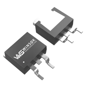
Whether replacing a competitor's medium-voltage SOP-8 dual MOSFET or sourcing high-current TO-263 devices for industrial battery systems, our technical support engineers provide detailed simulations and parametric comparisons. This reduces product development risks and shortens the design cycle.

Precision Wafer Testing Layout
BMS Testing Laboratory

Our Continuous Quality Commitment

Quality control is integrated into every step of Olukey's processes, from silicon wafer selection to final visual inspection of the package leads. Standard inspection flows include automated optical inspection (AOI) after die attach, wire bond pull testing, and 100% automated electrical testing of critical parameters like gate leakage, threshold voltage, and on-state resistance.

We supply high-reliability electronic components by partnering directly with semiconductor foundries. Our QA processes conform to global distribution standards, helping customers maintain consistent manufacturing yields.

Technical Q&A: BMS MOSFET Sourcing & Replacement

Expert insights regarding design considerations, parameter matching, and manufacturing standards.

What are the most critical parameters when cross-referencing a BMS MOSFET?

Beyond matching the drain-source breakdown voltage ($V_{DS}$) and continuous drain current ($I_D$), you must match the gate-source threshold voltage ($V_{GS(th)}$) to ensure compatibility with the existing gate driver circuit. Next, match the maximum $R_{DS(on)}$ at the target drive voltage to prevent overheating. Finally, check the gate charge ($Q_g$ and $Q_{gd}$) to maintain equivalent switching speeds, and confirm the thermal resistance ($R_{\theta JC}$) of the package to prevent heat build-up on the PCB.

Why is SGT (Split-Gate Trench) technology preferred over planar designs in high-current BMS?

SGT technology features a shielded gate electrode that reduces the gate-to-drain capacitance ($C_{gd}$), resulting in lower gate charge ($Q_g$) and faster switching speeds. Crucially, SGT reduces the specific on-state resistance per unit area, enabling sub-milliohm $R_{DS(on)}$ values in small surface-mount packages. This helps reduce power dissipation in high-current battery systems.

How does Olukey ensure parameter consistency when using parallel MOSFET arrays in large battery packs?

Our wafer manufacturing partners use advanced statistical process controls (SPC) to minimize batch-to-batch variation. We ensure tight tolerances for threshold voltage ($V_{GS(th)}$) and on-state resistance ($R_{DS(on)}$). This parameter matching prevents current imbalances among parallel devices, reducing the risk of localized hot spots.

What lead times and supply assurance measures does Hongkong Olukey offer?

Olukey works directly with major semiconductor foundries to maintain buffer stocks of raw wafers and popular packages (like DFN5x6 and TO-263). This approach helps protect customers from global supply shocks, allowing us to maintain standard lead times of 4 to 8 weeks, compared to the longer lead times of some overseas manufacturers.

How do I verify the thermal performance of a replacement MOSFET?

Start by comparing the junction-to-case thermal resistance ($R_{\theta JC}$) on the datasheet. Then, run thermal simulations under maximum continuous and peak transient currents. We recommend testing the replacement components on a prototype PCB under worst-case environmental conditions, using an infrared camera to check for hot spots and verify thermal performance.

Semi-conductor Wafer Production Lab