Direct drop-in equivalents and custom component solutions engineered for advanced battery protection, power control circuits, and intelligent microprocessing.
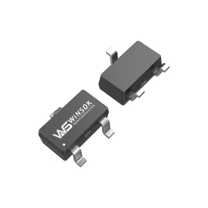


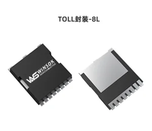
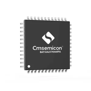
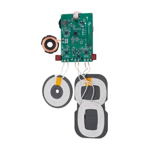
As a global, high-value solution provider, we focus on delivery excellence across three foundational product pillars: WINSOK MOSFETs, Cmsemicon MCUs, and bespoke PCBA circuit board solution development. Standing at the intersection of quality and economic feasibility, we specialize in offering high-reliability semiconductor cross-references that allow engineering and procurement teams to bypass global supply chain volatility.
By leveraging strategic ties with world-class wafer fabricators and packaging houses, we provide advanced alternative components designed to replace hard-to-source parts. Whether you are aiming to source equivalents for battery pack protection, mobile chargers, industrial battery management systems (BMS), or automotive assemblies, our engineering capabilities guarantee drop-in safety, optimized FOM (Figure of Merit), and substantial overall cost reduction.



Critical design requirements for modern Battery Management Systems (BMS) emphasizing RDS(on), thermal management, and reliable transient handling.
In Lithium-ion, Lithium Iron Phosphate (LiFePO4), and next-generation polymer batteries, the protection circuit module (PCM) or Battery Management System (BMS) serves as the primary barrier against failure. Overcharge, overdischarge, short-circuits, and thermal runaway hazards can cause destructive thermal incidents. High-performance, low-power-loss MOSFETs serve as the critical control switches in these safety circuits.
When engineering teams search for drop-in equivalent MOSFETs to mitigate supply shortages or control costs, simple parameter matching is insufficient. Design integrity requires detailed evaluation of several parameters:
| Parameters to Match | Standard Specs (BMS) | Why it Matters | Winsok Solutions |
|---|---|---|---|
| $V_{DS}$ (Breakdown Voltage) | 12V to 100V | Provides safety margin against voltage surges during switch-off. | Full coverage with 20V, 30V, 40V, 60V, 100V options. |
| $R_{DS(on)}$ (At 4.5V Gate Drive) | < 1.5 mΩ to 20 mΩ | Determines continuous current carrying capacity and thermal limits. | Ultra-low RDS(on) utilizing advanced trench process tech. |
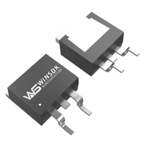
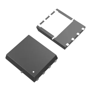
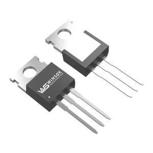
| $I_D$ (Continuous Current) | 5A to 150A+ | Must match battery pack maximum discharge rating. | Comprehensive scale from DFN2x2 up to TO-263 and TO-220 packages. |
| $V_{GS(th)}$ | 0.8V to 2.5V | Logic compatibility with protection ICs. | Sub-threshold turn-on optimized for single-cell applications. |
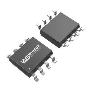
In portable electronics and e-mobility designs, board real estate is highly constrained. Traditional SOP-8 packages are increasingly replaced by DFN3X3-8, DFN5X6-8, and DFN2x2 packages. The leadless, exposed thermal pad design of DFN packaging reduces thermal resistance ($R_{\theta JC}$) by over 50% compared to leaded packages, allowing higher power handling in smaller footprints.
Evaluating cost optimization, production capacity, and global delivery security in the modern power electronics landscape.
Shenzhen and the wider Greater Bay Area house the world's most dense cluster of wafer fabs, packaging facilities, testing houses, and raw material suppliers. This reduces logistics overhead, minimizes production lead times, and accelerates prototyping.
By combining competitive domestic supply chains with strict global testing protocols (HTRB, HTGB, Temperature Cycling, and ESD protection testing), we deliver alternative components that meet international reliability guidelines.
We bypass the 26-to-52 week lead times of traditional Tier-1 semiconductor conglomerates. By maintaining strong inventory positions of wafers and raw packaging materials, our supply chain ensures steady 4-to-8 week delivery schedules.

Our solutions adapt to the diverse operational profiles and load dynamics of various electronics sectors.
Residential solar backup systems and utility-scale energy storage require robust BMS designs to handle cell imbalances and massive energy transfers. Our high-voltage MOSFETs (100V to 150V in TO-220 or TO-263 packages) protect these storage systems against current surges and over-discharge cycles.
From electric scooters and e-bikes to advanced driver-assistance systems (ADAS), high ambient temperatures and severe vibrations are constant challenges. Our rugged MOSFET lines feature low thermal resistance, high junction temperatures ($T_j = 175^\circ\text{C}$), and high ESD tolerance to ensure functional safety.
Smartphones, wearables, and wireless smart home sensors require small footprints. Dual N-channel or common-drain CSP configurations are utilized to fit into small form factors. Low gate threshold levels allow direct drive from low-voltage microcontrollers to maximize power savings.


Bridging the gap between component shortages, quality mandates, and cost reduction goals.
Modern supply chain managers face a difficult choice: stick with major global semiconductor brands and risk long lead times, or seek equivalent alternatives with the challenge of verifying quality. We solve this trade-off by offering structured cross-referencing, free engineering evaluation samples, and complete traceability.
Our experienced engineering team can cross-reference major product series from companies like Infineon, ON Semi, AOS, Vishay, and Nexperia. Clients receive a comprehensive comparison sheet detailing parameters like $R_{DS(on)}$, $Q_g$, $V_{GS(th)}$, and thermal dissipation metrics ($R_{\theta JC}$), alongside a layout pinout analysis to ensure compatibility.
To eliminate procurement risk, we supply free samples for board-level testing. This allows your team to perform validation checks, including load transient sweeps, thermal imaging under full operational load, and short-circuit protection speed testing.
Through our established wafer foundry relationships, we can scale production from initial prototype runs to monthly shipments of millions of units. We maintain inventory buffers of key wafers to absorb market demand spikes and ensure consistent supply.
Delivering high-quality electronic components and design services to support manufacturing requirements worldwide.
Over the years, our business model has relied on reputation to survive, adhering to the core tenet of "quality first, service first". We have established deep cooperative relationships with many high-tech enterprises and original manufacturers at home and abroad. By active market development and resource integration, we have grown into a reliable semiconductor distributor in the Asia-Pacific region.
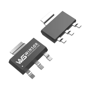
The WINSOK MOSFET portfolio covers a wide range of low and medium-voltage requirements: 15V, 20V, 30V, 40V, 60V, 80V, 100V, 120V, 150V, 200V, 250V, 300V, 400V, 500V, 600V, 650V. Packages include:
With more than 600 models and over 40 package styles, our product range covers the majority of low-to-medium voltage MOSFET applications currently on the market. Furthermore, our partnership with Cmsemicon MCU provides access to robust 8-bit and 32-bit microcontrollers, allowing us to supply complete system-level solutions that integrate power conversion, control logic, and protection.

Addressing common queries from electronic engineers, procurement teams, and product managers.
Explore our additional high-reliability N-channel and P-channel MOSFETs designed for battery management, load switching, and motor control applications.

 Olukey