Olukey
1 / 1
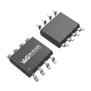
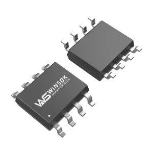
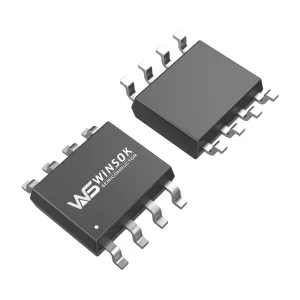
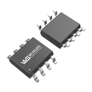
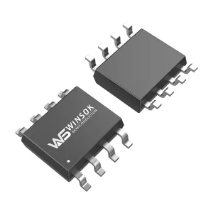
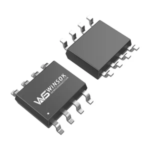
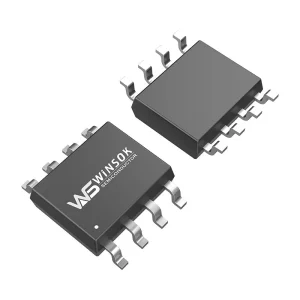
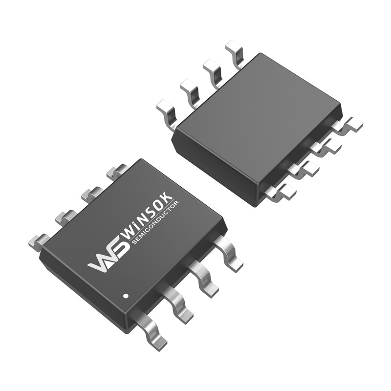
The WSP6067A MOSFETs are the most advanced for trench P-ch technology, with a very high density of cells. They deliver excellent performance in terms of both the RDSON and gate charge, suitable for most synchronous buck converters. These MOSFETs meet RoHS and Green Product criteria, with 100% EAS guaranteeing full functional reliability.
Advanced technology enables high-density cell trench formation, resulting in super low gate charge and superior CdV/dt effect decay. Our devices come with a 100% EAS warranty and are environmentally friendly.
High density of cells for optimized power delivery.
Minimizes conduction loss to improve overall efficiency.
Ensuring complete functional reliability and robustness.
| Symbol | Parameter | Rating (N-Ch / P-Ch) | Units | |
|---|---|---|---|---|
| VDS | Drain-Source Voltage | 60 | -60 | V |
| VGS | Gate-Source Voltage | ±20 | ±20 | V |
| ID @ TC=25℃ | Continuous Drain Current, VGS @ 10V1 | 7.0 | -5.0 | A |
| ID @ TC=100℃ | Continuous Drain Current, VGS @ 10V1 | 4.0 | -2.5 | A |
| IDM | Pulsed Drain Current2 | 28 | -20 | A |
| EAS | Single Pulse Avalanche Energy3 | 22 | 28 | mJ |
| IAS | Avalanche Current | 21 | -24 | A |
| PD @ TC=25℃ | Total Power Dissipation4 | 2.0 | 2.0 | W |
| TSTG | Storage Temperature Range | -55 to 150 | ℃ | |
| TJ | Operating Junction Temperature Range | -55 to 150 | ℃ | |
| Symbol | Parameter | Conditions | Min. | Typ. | Max. | Unit |
|---|---|---|---|---|---|---|
| BVDSS | Drain-Source Breakdown Voltage | VGS=0V , ID=250uA | 60 | --- | --- | V |
| △BVDSS/△TJ | BVDSS Temperature Coefficient | Reference to 25℃ , ID=1mA | --- | 0.063 | --- | V/℃ |
| RDS(ON) | Static Drain-Source On-Resistance2 | VGS=10V , ID=5A | --- | 38 | 52 | mΩ |
| VGS=4.5V , ID=4A | --- | 55 | 75 | |||
| VGS(th) | Gate Threshold Voltage | VGS=VDS , ID =250uA | 1 | 2 | 3 | V |
| △VGS(th) | VGS(th) Temperature Coefficient | --- | -5.24 | --- | mV/℃ | |
| IDSS | Drain-Source Leakage Current | VDS=48V , VGS=0V , TJ=25℃ | --- | --- | 1 | uA |
| VDS=48V , VGS=0V , TJ=55℃ | --- | --- | 5 | |||
| IGSS | Gate-Source Leakage Current | VGS=±20V , VDS=0V | --- | --- | ±100 | nA |
| gfs | Forward Transconductance | VDS=5V , ID=4A | --- | 28 | --- | S |
| Rg | Gate Resistance | VDS=0V , VGS=0V , f=1MHz | --- | 2.8 | 4.3 | Ω |
| Qg | Total Gate Charge (4.5V) | VDS=48V , VGS=4.5V , ID=4A | --- | 19 | 25 | nC |
| Qgs | Gate-Source Charge | --- | 2.6 | --- | ||
| Qgd | Gate-Drain Charge | --- | 4.1 | --- | ||
| Td(on) | Turn-On Delay Time | VDD=30V , VGS=10V , RG=3.3Ω, ID=1A | --- | 3 | --- | ns |
| Tr | Rise Time | --- | 34 | --- | ||
| Td(off) | Turn-Off Delay Time | --- | 23 | --- | ||
| Tf | Fall Time | --- | 6 | --- | ||
| Ciss | Input Capacitance | VDS=15V , VGS=0V , f=1MHz | --- | 1027 | --- | pF |
| Coss | Output Capacitance | --- | 65 | --- | ||
| Crss | Reverse Transfer Capacitance | --- | 45 | --- |
The WSP6067A MOSFET utilizes advanced trench P-channel technology with a very high cell density to offer superior performance in gate charge and on-resistance.
It is widely used in high frequency point-of-load synchronous buck converters, DC-DC power systems, load switches, drones, medical equipment, car chargers, wireless charging, and consumer electronics.
The 100% EAS (Equivalent Avalanche Single-Pulse) guarantee ensures that the MOSFET is fully tested and capable of handling specified transient energy pulses, verifying overall system reliability.
Yes, these MOSFET devices fully meet RoHS and Green Product criteria, meaning they are lead-free and free of hazardous substances.
The operating junction temperature (TJ) and storage temperature (TSTG) ranges are rated from -55℃ to 150℃, making it suitable for tough environments.