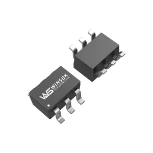
Automotive-grade switching components optimized for power factor correction (PFC) and resonant stages. Request your free sample today.



Under the lens of automotive system design, high-frequency conversion efficiency and thermal management are the primary drivers of next-generation MOSFET packaging and design paradigms.
An On-Board Charger (OBC) is a critical subsystem in hybrid and pure battery electric vehicles. It converts an external AC source (from domestic or public charging stations) into direct current (DC) to charge the high-voltage battery. Because space, weight, and volume inside the vehicle are highly restricted, automotive designers continuously strive for high power density. This optimization is largely driven by switching frequencies and efficiency improvements inside the converter topology.
Traditional silicon planar MOSFETs are reaching their theoretical physical limits. Modern OBC designs rely heavily on Superjunction (SJ) Silicon MOSFETs and Silicon Carbide (SiC) Wide-Bandgap (WBG) technology. Replacing failing or obsolete MOSFETs within these chargers requires parts with extremely low gate charge ($Q_g$), reduced static drain-source on-state resistance ($R_{DS(on)}$), and robust avalanche energy capacity ($E_{AS}$).
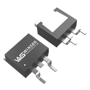
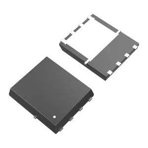
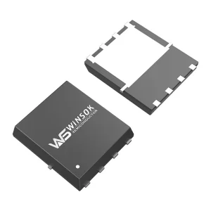
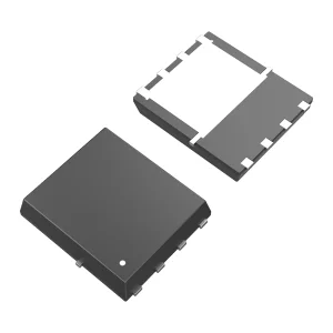
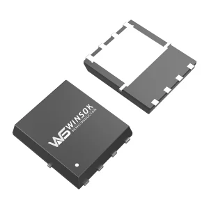
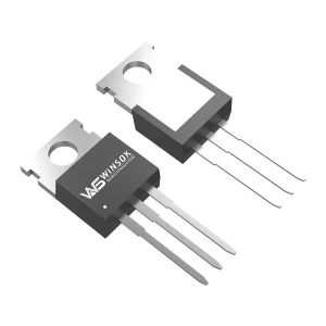
Evaluating standard data sheets does not tell the whole story. Design engineers require concrete physical parameters during the replacement cycle. Replacing legacy components (like older generation TO-220 or TO-263 packages) with modern, low-parasitic surface-mount packages such as the DFN5X6-8 or DFN8X8 reduces parasitic source inductance significantly. This minimization directly affects voltage ringing and allows for faster gate switching speeds without exceeding maximum ratings.
Evaluating component characteristics under rigorous operating conditions.
The global automotive power semiconductor market is undergoing a transition from traditional 400V battery architectures to ultra-fast charging 800V architectures. Consequently, On-Board Chargers must accommodate wider input and output voltage ranges, placing extreme switching stress on primary and secondary-side power switches.
Key industrial trends in the OBC MOSFET manufacturing supply chain include:

Adapting high-performance MOSFET configurations to varied operating conditions and structural profiles.
OBCs installed in electric vehicles operating in sub-zero or high-humidity regions face thermal shock. Under these scenarios, MOSFETs must withstand rapid gate driver signal propagation down to -40°C while maintaining stable threshold voltage values ($V_{GS(th)}$) to avoid premature conduction.
Forklifts, harbor logistics trucks, and delivery vehicles run round-the-clock shift patterns. Replacement MOSFETs in these applications must prioritize low switching losses ($E_{on}$ and $E_{off}$) during continuous operation at variable power factors.
Charging electric vehicles using off-grid microgrids introduces high input voltage transients. Using medium-to-high voltage MOSFETs (up to 650V rated) with robust avalanche ratings prevents catastrophic over-voltage failures.
Integrating components, controller processing, and circuit board design into complete electronic solutions.
HONGKONG Olukey INDUSTRY CO., LIMITED is a solution provider focusing on the overall solution of electronic product components. The main products mainly include: WINSOK MOSFET, Cmsemicon MCU, PCBA circuit board solution development and other three types of product lines.
At present, the products of Olukey Industry are widely used in automotive electronics, military electronics, smart industry, new energy, smart medical care, 5G, Internet of Things, smart home, and various consumer electronics products. Relying on the advantages of global general agents of major original factories, we are based in the Asia-Pacific market. Provide customers with various advanced high-tech electronic components by using comprehensive superior services, assist manufacturers in producing high-quality products and provide comprehensive services.
Relying on the advantages of global general agents of major original manufacturers, we are based on the Asia-Pacific market. Through active market development and effective resource integration, it has become one of the outstanding and fast-growing agents in the Asia-Pacific region. The company has many years of professional distribution experience. We use our comprehensive advantageous services to provide customers with various types of advanced high-tech electronic components, assist manufacturers in producing high-quality products and provide comprehensive services.




We use comprehensive high-quality services to provide customers with various types of advanced high-tech electronic components, assist manufacturers in producing high-quality products and provide comprehensive services. Over the years, the company has relied on reputation to survive, adhering to the tenet of "quality first, service first", and has established good cooperative relationships with many high-tech enterprises and original manufacturers at home and abroad.
WINSOK MOSFET's product voltages are mainly medium and low voltage: 15V, 20V, 30V, 40V, 60V, 80V, 100V, 120V, 150V, 200V, 250V, 300V, 400V, 500V, 600V, 650V.
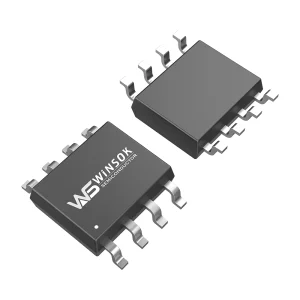
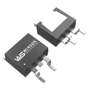
The main packages include DFN3X3-8, DFN5X6-8, TO-252, TO-263, SOP-8, SOT-23, TO-220, etc. There are more than 600 models and more than 40 packages. Extensive coverage of medium-voltage and low-voltage MOSFET product lines on the market.
Cmsemicon MCU is a microcontroller company born in Shenzhen, with rich product types and technology research and development experience. Becoming a global high-value agent is the common goal pursued by OLUKEY Industrial employees. We work hand in hand with suppliers to jointly explore a larger market and contribute to the prosperity and development of semiconductors.

Providing actionable technical answers to critical engineering design questions.

Explore our full line of automotive and industrial packages, featuring various current levels and low conduction losses.
 Olukey