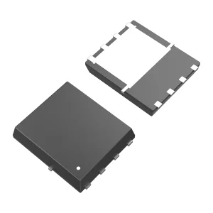
Analyzing global semiconductor supply pathways, performance parameters, and the rise of high-performance replacement protocols for battery management systems.
The global battery system market is undergoing an unprecedented expansion, driven by the electrification of mobility, the deployment of industrial utility-scale energy storage systems (ESS), and the scaling of telecom infrastructures. At the heart of every Battery Management System (BMS) lies the solid-state switching matrix—predominantly controlled by power MOSFETs. As supply chains face geopolitical stresses and capacity crunches, engineering and purchasing departments are moving away from single-source reliance.
This technical guide details the strategies for integrating high-reliability OEM Power MOSFET alternatives for BMS applications. We explore key performance indicators (KPIs) such as static drain-source on-resistance ($R_{DS(ON)}$), total gate charge ($Q_g$), thermal resistance ($R_{thJC}$), and avalanche ruggedness ($E_{AS}$). By utilizing qualified alternative silicon solutions, global hardware manufacturers can secure supply lines, lower production costs, and maintain parity or superior performance relative to legacy tier-1 components.
Direct supply line replacements for low-to-medium voltage configurations. Optimized for cell balancing, charge-discharge protection, and isolated power distribution.
Bridging advanced high-tech electronic component manufacturers with international application engineers.

HONGKONG Olukey INDUSTRY CO., LIMITED is a comprehensive solutions provider focusing on the overall distribution and design-in of premium electronic components. Our principal operation spans across three core product portfolios: WINSOK MOSFETs, Cmsemicon MCUs, and customized PCBA circuit board solutions.
Currently, our products are widely deployed in sectors requiring stringent operational reliability, including automotive electronics, defense-grade micro-systems, smart industrial controls, new energy management systems, critical medical devices, 5G communications infrastructure, IoT modules, smart home architectures, and high-performance consumer electronic products.
By leveraging global direct-agent partnerships with tier-1 and highly competitive original factories, we maintain a robust footprint in the Asia-Pacific market. We assist global original equipment manufacturers (OEMs) and electronic manufacturing services (EMS) providers in developing highly cost-effective, zero-defect power stages.
Why Tier-1 product managers and hardware designers trust Winsok and Olukey Industry for substitute validation.
We combine comprehensive, high-quality engineering services with an extensive semiconductor supply network. Over years of development, we have secured long-term stability by operating under a strict "quality first, service first" framework. Our deep-seated collaborations with regional fab facilities and testing houses allow us to bypass typical distribution markups.
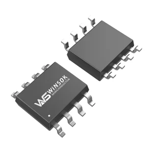
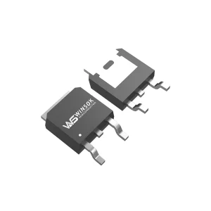
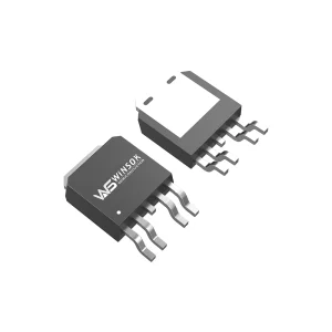
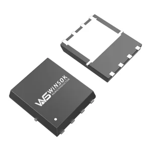
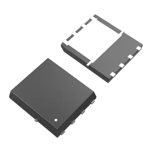
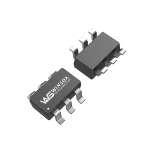
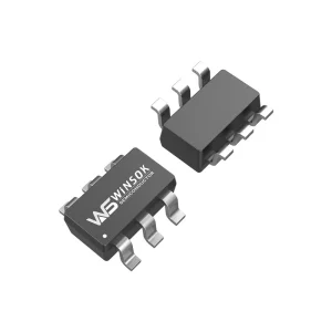
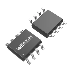
The WINSOK MOSFET product line spans an exceptionally wide voltage spectrum: 15V, 20V, 30V, 40V, 60V, 80V, 100V, 120V, 150V, 200V, 250V, 300V, 400V, 500V, 600V, and 650V. These silicon designs are housed in industry-standard packages, including DFN3X3-8, DFN5X6-8, TO-252, TO-263, SOP-8, SOT-23, TO-220, and more. With over 600 distinct models and 40 package types, our products match major industry footprints, offering drop-in replacements for standard components.
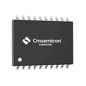
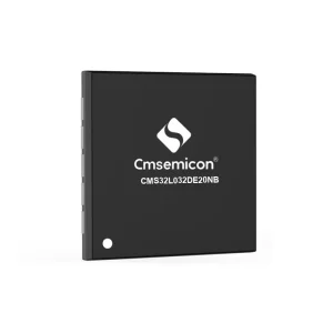
Complementing our power switches, Cmsemicon MCU products represent the apex of Shenzhen's high-reliability microcontroller research, supplying both 8-bit 8051 and 32-bit ARM Cortex-M0+ processing units (such as the CMS32L032 series) tailored for smart charge control and telemetry in modern BMS architectures.




Analyzing key market dynamics, supply chain constraints, and the shifting paradigms of semiconductor selection.
The transition toward sustainable energy ecosystems has accelerated the demand for high-capacity battery systems. Battery Management Systems (BMS) are the critical line of defense for these systems, regulating voltage, managing thermal profiles, and shielding the cells from overcharge, over-discharge, and thermal runaway. A core pillar of the BMS safety system is the Solid-State Switch—specifically the power MOSFET.
Historically, global OEMs relied heavily on a handful of top-tier Western semiconductor companies. However, global market trends are reshaping how procurement and design departments evaluate component sourcing:
How to cross-reference and qualify alternate MOSFETs against premium European, American, and Japanese brands.
Qualifying a power semiconductor replacement in a BMS protection circuit requires a detailed evaluation of electrical and thermal characteristics. Pin-to-pin similarity is only the first step. Below is the engineering roadmap used by validation engineers to verify functional equivalency:
| Critical Parameter | Relevance in BMS Protection | Risk Factor of Inadequate Alternatives | Winsok Equivalent Advantage |
|---|---|---|---|
| $R_{DS(ON)}$ (at $V_{GS}$ = 10V) | Determines continuous conduction loss ($I^2R$) and overall heat generation of the switch board. | Elevated $R_{DS(ON)}$ causes thermal build-up, leading to early thermal shutdown or system degradation. | Optimized Trench technology down to sub-1.5mΩ ranges in DFN5x6-8 and TO-263 packages. |
| $V_{GS(th)}$ (Gate Threshold Voltage) | Determines the voltage needed to turn the channel fully ON. Critical for MCU/driver interfacing. | If the threshold is too high, the MCU cannot turn the MOSFET fully on, leading to highly dissipative linear mode operation. | Consistent threshold limits with tight distribution tolerances, compatible with low-voltage driver outputs. |
| $Q_g$ & $Q_{gd}$ (Gate Charges) | Dictates switching speed and the current required from the gate driver during transitions. | High gate charge slows down switching speeds, leading to excessive switching losses during short-circuit events. | Low Miller charge ($Q_{gd}$) designs, enabling rapid turn-off under fault conditions. |
| $I_{DM}$ (Pulsed Drain Current) | Defines the peak pulse current the switch can safely pass before wire bond or die destruction. | Failure under inrush conditions when connecting to highly capacitive load blocks (e.g., inverters). | High cell-density design ensures superior pulsed current handling limits, verified via advanced UIS testing. |
In addition to active parameters, packaging thermal performance is a critical factor. For instance, replacing an international DFN5x6-8 MOSFET requires evaluating the internal leadframe attachment of the alternative factory. Winsok utilizes clip-bond technology rather than traditional wire bonding for high-current profiles. This reduces parasitic package inductance and optimizes the junction-to-case thermal resistance ($R_{thJC}$), allowing for higher continuous currents without violating safe operating parameters.
From micro-mobility to megawatt-scale industrial energy hubs—tailored layouts and silicon selections.
Operating under typical voltage profiles of 36V, 48V, and 72V, micro-mobility BMS boards require compact, low-RDS(on) components. The application of dual N-channel units like the WSP9926 or single N-channel switches in TO-252 (e.g., WSF30150) allows designers to integrate dual-side charging/discharging switches in tight enclosures without active heat-sinking.
These systems require continuous duty cycles under moderate to high load currents. Integrating high-current switches like the WSF30160 (N-channel 30V 160A) ensures low temperature rises on the BMS controller. When configured in parallel, these components handle charging profiles exceeding 100A continuously, matching standard industrial profiles.
These systems run on 48V nominal lines, but experience voltage spikes from inductances and switching events. High-voltage series alternatives, such as the WSP11N10T (Dual N-channel 100V), provide a safety margin against voltage transients. Pairing these switches with high-density microcontroller monitoring creates a reliable protection loop.
Why China's semiconductor packaging and testing clusters provide a strategic advantage for global buyers.
China's domestic semiconductor packaging and assembly infrastructure, particularly centered around the Pearl River Delta, has evolved from a high-volume manufacturing center into an advanced engineering hub. By working with alternatives from Shenzhen and Hong Kong, buyers can leverage several unique structural advantages:

Ensuring compliance with international standards for smooth global deployment.
Every product entering international markets must comply with local regulatory frameworks. Winsok alternatives comply with the following standards:
One of the primary challenges when validating an alternative components vendor is the lack of direct engineering support. OLUKEY Industry addresses this by offering dedicated Field Application Engineering (FAE) support. We assist customer engineering departments with:
Addressing design questions, pin compatibility concerns, and testing requirements.
Engineers must compare maximum drain-source voltage ($V_{DS}$), continuous and pulsed drain current ($I_D$/$I_{DM}$), gate threshold voltage ($V_{GS(th)}$), and drain-source on-resistance ($R_{DS(on)}$). Additionally, total gate charge ($Q_g$) must be evaluated to ensure the existing gate driver can drive the replacement without overheating or causing excessive switching losses.
Dual N-channel packages (such as the SOP-8 housed WSP9926) integrate two independent silicon dies within a single package footprint. This configuration is common in low-voltage, low-current battery systems (like smart home sensors or small power banks) to save board space, whereas high-power systems utilize separate single N-channel devices in packages like DFN5x6 or TO-263 to manage thermal dissipation.
$R_{DS(on)}$ rises as the junction temperature increases. When selecting an alternative MOSFET, it is critical to verify the resistance curve up to the maximum operating junction temperature (typically 150°C or 175°C) to prevent thermal runaway under full load conditions.
For high-vibration applications, surface mount packages with low profile parameters, such as DFN5x6-8 or DFN3x3-8, are preferred over through-hole packages. They offer lower parasitic inductance and a low-profile construction that reduces mechanical stress on solder joints during shock events.
Yes. Olukey Industry offers reference designs that pair Cmsemicon microcontrollers (such as the 8-bit CMS8S5885 or the 32-bit CMS32L032) with Winsok MOSFETs. The MCU manages analog-front-end telemetry and executes cell-balancing and protection logic, while the MOSFETs act as the switching elements.
Designed for multi-cell pack configurations, high-voltage battery banks, and intelligent management microcontrollers.

The trend towards higher integration, wide-bandgap semiconductors, and intelligent protection topologies.
Looking ahead, the development of BMS power switches is focused on further reducing $R_{DS(on)}$ and package dimensions. While conventional silicon (Si) trench processes are approaching their theoretical limits, packaging innovations continue to drive improvement. High-current packages like the DFN8x8 and toll-type footprints are increasingly adopted to replace through-hole TO-220 packages, enabling automated assembly lines and reducing parasitic inductance.
Additionally, wide-bandgap (WBG) materials, specifically Gallium Nitride (GaN) and Silicon Carbide (SiC), are emerging in high-voltage battery storage systems (exceeding 400V). In these high-power profiles, the low switching losses of GaN enable high-frequency operation, reducing the size of filters and passive components on the BMS board.
Simultaneously, the industry is moving toward smart power switches that integrate gate drivers, level shifters, and diagnostic systems onto a single die. These devices provide real-time telemetry on load current, die temperature, and gate status directly to the central MCU, facilitating predictive maintenance and thermal balancing.

 Olukey