Olukey
1 / 1
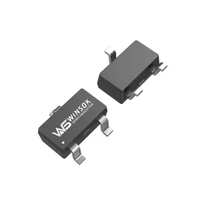
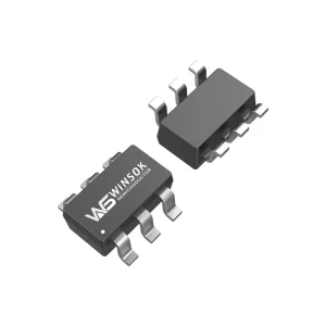
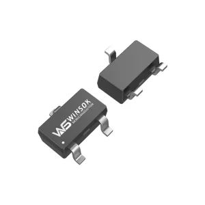
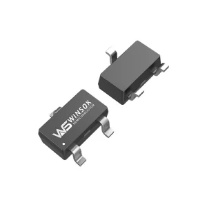
The WST2011 MOSFETs are the most advanced P-ch transistors available, featuring unrivaled cell density. They offer exceptional performance, with low RDSON and gate charge, making them ideal for small power switching and load switch applications. Furthermore, the WST2011 meets RoHS and Green Product standards and boasts full-function reliability approval.
Designed for higher cell density, enabling an optimized and highly efficient Green Device structure.
Delivers excellent CdV/dt effect decline and exceptionally low RDSON resistance values.
| Symbol | Parameter | Rating | Units | |
| 10s | Steady State | |||
| VDS | Drain-Source Voltage | -20 | V | |
| VGS | Gate-Source Voltage | ±12 | V | |
| ID@TA=25℃ | Continuous Drain Current, VGS @ -4.5V1 | -3.6 | -3.2 | A |
| ID@TA=70℃ | Continuous Drain Current, VGS @ -4.5V1 | -2.6 | -2.4 | A |
| IDM | Pulsed Drain Current2 | -12 | A | |
| PD@TA=25℃ | Total Power Dissipation3 | 1.7 | 1.4 | W |
| PD@TA=70℃ | Total Power Dissipation3 | 1.2 | 0.9 | W |
| TSTG | Storage Temperature Range | -55 to 150 | ℃ | |
| TJ | Operating Junction Temperature Range | -55 to 150 | ℃ | |
| Symbol | Parameter | Conditions | Min. | Typ. | Max. | Unit |
| BVDSS | Drain-Source Breakdown Voltage | VGS=0V , ID=-250uA | -20 | --- | --- | V |
| △BVDSS/△TJ | BVDSS Temperature Coefficient | Reference to 25℃ , ID=-1mA | --- | -0.011 | --- | V/℃ |
| RDS(ON) | Static Drain-Source On-Resistance2 | VGS=-4.5V , ID=-2A | --- | 80 | 85 | mΩ |
| VGS=-2.5V , ID=-1A | --- | 95 | 115 | |||
| VGS(th) | Gate Threshold Voltage | VGS=VDS , ID =-250uA | -0.5 | -1.0 | -1.5 | V |
| △VGS(th) | VGS(th) Temperature Coefficient | Reference to 25℃ | --- | 3.95 | --- | mV/℃ |
| IDSS | Drain-Source Leakage Current | VDS=-16V , VGS=0V , TJ=25℃ | --- | --- | -1 | uA |
| VDS=-16V , VGS=0V , TJ=55℃ | --- | --- | -5 | |||
| IGSS | Gate-Source Leakage Current | VGS=±12V , VDS=0V | --- | --- | ±100 | nA |
| gfs | Forward Transconductance | VDS=-5V , ID=-2A | --- | 8.5 | --- | S |
| Qg | Total Gate Charge (-4.5V) | VDS=-15V , VGS=-4.5V , ID=-2A | --- | 3.3 | 11.3 | nC |
| Qgs | Gate-Source Charge | --- | 1.1 | 1.7 | ||
| Qgd | Gate-Drain Charge | --- | 1.1 | 2.9 | ||
| Td(on) | Turn-On Delay Time | VDD=-15V , VGS=-4.5V , RG=3.3Ω, ID=-2A | --- | 7.2 | --- | ns |
| Tr | Rise Time | --- | 9.3 | --- | ||
| Td(off) | Turn-Off Delay Time | --- | 15.4 | --- | ||
| Tf | Fall Time | --- | 3.6 | --- | ||
| Ciss | Input Capacitance | VDS=-15V , VGS=0V , f=1MHz | --- | 750 | --- | pF |
| Coss | Output Capacitance | --- | 95 | --- | ||
| Crss | Reverse Transfer Capacitance | --- | 68 | --- |
High frequency point-of-load synchronous small power switching is suitable for use in MB/NB/UMPC/VGA, networking DC-DC power systems, load switches, e-cigarettes, controllers, digital products, small household appliances, and consumer electronics.