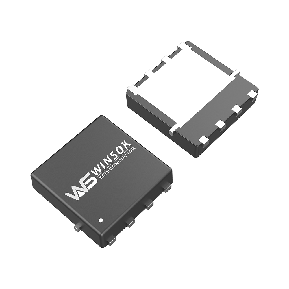
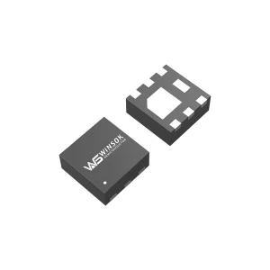
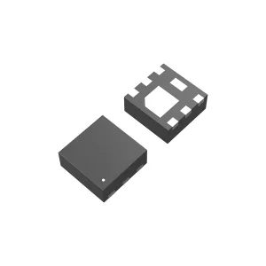
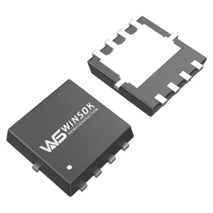
The WSD2209DN33 is a high-performance Dual P-channel MOSFET designed for efficient power management and switching applications. Boasting a compact form factor with low on-resistance, this MOSFET delivers reliable performance in space-constrained electronic designs.
What are the key ratings of the WSD2209DN33 MOSFET?
The WSD2209DN33 MOSFET features a drain-source voltage (VDS) of -20V, a continuous drain current (ID) of -7.5A, and a typical on-resistance (RDS(ON)) of 28mΩ at 4.5V.
What type of configuration and package does WSD2209DN33 use?
This MOSFET is structured in a Dual P-channel configuration and is housed in a compact DFN3X3-8L package, which allows for high density board layouts.
What is the gate-to-source voltage (VGS) for WSD2209DN33?
The gate-to-source voltage (VGS) rating for the WSD2209DN33 MOSFET is ±10V.
In which applications is the WSD2209DN33 commonly used?
It is commonly utilized in electronic cigarettes, wireless chargers, car chargers, controllers, digital products, small household appliances, and various consumer electronics.
What are the on-resistance values at different gate voltages?
The typical and maximum on-resistance (RDS(ON)) values are: 28mΩ (Typ) / 33mΩ (Max) at 4.5V, 37mΩ (Typ) / 45mΩ (Max) at 2.5V, and 50mΩ (Typ) / 68mΩ (Max) at 1.8V.
What is the input capacitance (Ciss) of the WSD2209DN33?
The input capacitance (Ciss) for the WSD2209DN33 is 1160 pF, supporting efficient high-speed switching operations.
 Olukey