Global BMS Design-in & Replacement Solutions

China Power MOSFET for BMS Cross Reference Suppliers & Factories

Industrial Whitepaper: Navigating BMS Power MOSFET Sourcing & Cross-Referencing

Executive Summary: As global energy transition accelerates, Battery Management Systems (BMS) have emerged as the primary guardian of cell longevity and operation safety. Power MOSFETs serve as the crucial electronic switchgear within these systems. Ensuring a reliable, cost-efficient, and multi-source supply chain via high-precision cross-referencing has transitioned from an operational option to a core strategic necessity.

1. The Evolution of Battery Management Systems & MOSFET Demands

Modern Battery Management Systems (BMS) do much more than basic voltage monitoring. In applications ranging from consumer light electric vehicles (LEVs) to large-scale industrial Energy Storage Systems (ESS) and electric vehicle (EV) powertrains, a BMS is responsible for cell balancing, state-of-charge (SoC) estimation, state-of-health (SoH) diagnostics, and comprehensive over-current/thermal runaway prevention.

Within this ecosystem, the power MOSFET acts as the execute-to-protect gatekeeper. During normal operations, it must pass high continuous current with minimal conduction loss (governed by $R_{DS(ON)}$). During fault conditions—such as short circuits or charging surges—it must switch off within microseconds to isolate the pack, bearing massive transient avalanche energies. The demand for sub-milliohm resistance, low gate charge ($Q_g$), and enhanced Safe Operating Areas (SOA) has positioned MOSFET design as a cornerstone of modern power electronics engineering.

600+
MOSFET Models
40+
Package Options
15V-650V
Voltage Range
< 1ms
Fault Response

2. Sourcing Resilience: Why BMS Cross-Reference Engineering is Essential

For procurement managers and hardware design engineers, sole-sourcing high-power components presents significant supply chain vulnerabilities. Geopolitical shifts, wafer allocation shortages, and logistics disruptions can halt production. Implementing a robust "pin-to-pin" cross-referencing framework with premium alternative suppliers is critical.

A professional cross-reference process evaluates electrical characteristics beyond nominal Vds and Id. It requires analyzing:

  • Thermal Resistance ($R_{thJC}$): Ensuring the package can dissipate heat effectively under heavy loads.
  • Gate Threshold Voltage ($V_{GS(th)}$): Securing compatibility with the driving outputs of the microcontroller (MCU) or analog front end (AFE) without additional gate driver circuitry modifications.
  • Body Diode Reverse Recovery ($Q_{rr}$ & $t_{rr}$): Critical for minimizing switching noise and EMI during high-frequency balancing operations.

3. Corporate Profile: HONGKONG Olukey INDUSTRY CO., LIMITED

HONGKONG Olukey INDUSTRY CO., LIMITED is a leading solution provider focusing on the overall integration and supply of electronic product components. Our main portfolio consists of three pillar product lines: WINSOK MOSFET, Cmsemicon MCU, and custom PCBA circuit board solution development.

Currently, Olukey Industry's components and systems are deployed across automotive electronics, military systems, smart industrial controls, new energy ecosystems, advanced medical devices, 5G communication infrastructure, the Internet of Things (IoT), smart home appliances, and consumer electronics. Harnessing the structural advantage of global distribution partnerships with major original factories, we support the Asia-Pacific and global markets with high-reliability semiconductor sourcing and technical services.

Olukey Industrial Semiconductor Solutions

4. Comprehensive Cross-Reference Substitution Guide

By cooperating with Olukey, engineers have access to a massive database of drop-in equivalents to Tier-1 Western and East Asian brands. This minimizes design cycle times and avoids expensive PCB redesigns.

Industry Standard Part Winsok Equivalent Part Package Key Specifications Status / Direct Cross
AOS AON6512 WSD30150DN56 DFN5X6-8 N-Channel 30V 150A, Ultra-Low RDS(on) Pin-to-Pin Direct
Panjit PJQ5428 WSD4070DN33 DFN3X3-8L N-Channel 40V 68A, High Avalanche Ruggedness Compatible Design
AOS AONS3234 WSD3039DN56 DFN5X6-8L N+P Complementary Pair, Optimized Gate Charge Direct Cross
Infineon BSC010N04LS WSK200N08 / WSK96N08 TO-263-2L High-Power 80V 200A/96A, Low Thermal Drift Premium Alt

5. Technological Advantages of Winsok MOSFETs in BMS Applications

Winsok MOSFET’s product voltages are mainly focused on medium and low-voltage applications, bridging the standard requirements of multi-cell battery packs: 15V, 20V, 30V, 40V, 60V, 80V, 100V, 120V, 150V, 200V, 250V, 300V, 400V, 500V, 600V, 650V.

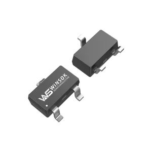
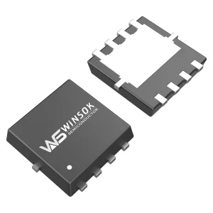
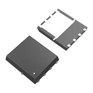
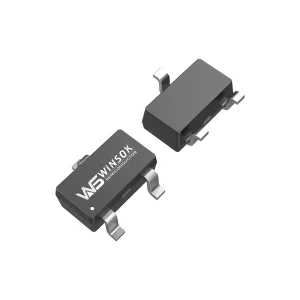
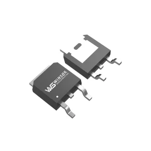
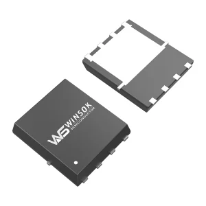
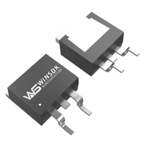
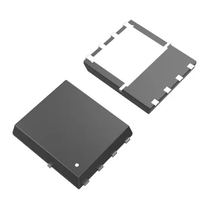
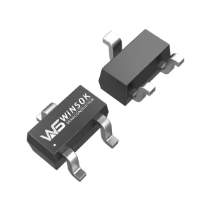
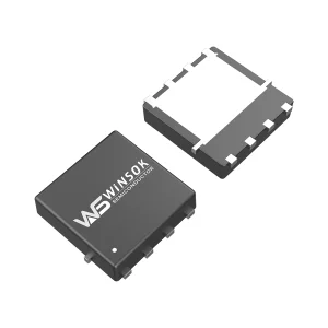
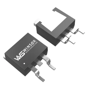
Our packages cover a wide range of mounting configurations: DFN3X3-8, DFN5X6-8, TO-252, TO-263, SOP-8, SOT-23, TO-220, and more. With over 600 models and 40 distinct package form-factors, we offer one of the most comprehensive replacement databases available on the market today.

Advanced Trench Gate & SGT Technology

Utilizing shielded gate trench (SGT) architectures to drastically reduce gate-to-drain charge ($Q_{gd}$) while maintaining industry-leading channel conduction efficiency.

Thermal Management Layouts

DFN packages are engineered with exposed thermal pads, delivering exceptionally low junction-to-case thermal impedance ($R_{thJC}$) for high-density layouts.

Robust Avalanche Safety (UIS)

Every batch of Winsok power devices undergoes 100% Unclamped Inductive Switching (UIS) testing to ensure resilience against inductive kickback spikes.

Precision MOSFET Packaging Line

6. Value-Added Design & Manufacturing Ecosystem

At Olukey, we understand that selecting a MOSFET is only one part of the equation. Modern BMS units require close coordination between the silicon switches, the processing unit, and the layout. By integrating Cmsemicon MCUs with Winsok MOSFETs, Olukey provides a turnkey approach:


  • Complete Firmware-Hardware Sync: Tailored code for MCU-driven protection loops matching the switching speeds of the output stage MOSFETs.
  • Prototyping & Production Design: Our in-house PCBA team designs power paths with optimum trace widths, minimizing parasitic inductance.
  • Rigorous Quality Control: Components are sourced directly from verified fabrication sites, ensuring batch-to-batch traceability.
Wafer Testing Diagnostics
SMT Board Assembly
Automated Optical Inspection
Semiconductor Quality Laboratory

7. Global Trends in Battery Management MOSFET Sourcing

The shift from traditional chemical cells to modern solid-state and high-energy-density lithium chemistries has put strict demands on BMS safety margins. Key global trends include:

  • High-Voltage Integration: The move from 12V-48V battery systems to 400V-800V layouts in EV/ESS installations has increased the demand for MOSFETs rated at 100V to 600V. High-voltage switching speeds and thermal control are more critical than ever.
  • Miniaturization and Copper-clip Packaging: Industry preference is shifting away from leaded TO-220 packages to advanced SMD types like DFN5x6 and TO-Leadless (Toll), which reduce footprint while maintaining high current capacity.
  • Automotive Compliance (AEC-Q101): Growing quality demand has driven factories to qualify their lines for automotive certification standards, ensuring lower failure rates (measured in Single Digit PPB).

8. Tech Roadmap: The Future of Power Switching in Energy Storage

As we approach 2026 and beyond, Olukey and Winsok are investing heavily in technologies that will define the next generation of BMS power stages. The focus remains on lowering the Figure of Merit ($FOM = R_{DS(on)} \times Q_g$). By optimizing the trench cell density and moving to thinner wafers, next-generation devices are projected to achieve a 15% reduction in conduction losses in the same footprint. This allows engineers to design smaller battery modules with increased safety margins and less cooling hardware.

Advanced Power MOSFET Wafer Technology

Technical Q&A - Frequently Asked Questions

Q1: How do I select the right cross-reference MOSFET for an existing BMS layout?
To select a cross-reference MOSFET, start by matching the package type (e.g., DFN5X6-8, TO-252) and the source-drain voltage rating ($V_{DS}$). Next, verify that the replacement’s $R_{DS(on)}$ at your design gate voltage ($V_{GS}$) is equal to or lower than the original part to avoid overheating. Finally, confirm that the gate charge ($Q_g$) is compatible with the drive current output of your BMS control circuit.
Q2: Why are Winsok MOSFETs considered reliable equivalents to tier-1 Western brands?
Winsok products are manufactured on modern fabrication lines utilizing state-of-the-art Shielded Gate Trench (SGT) technology. This achieves electrical parameters ($FOM$, switching loss) matching or exceeding major industry standards, but with improved supply chain stability and shorter lead times.
Q3: What is the significance of the body diode properties in a BMS switch?
In BMS circuits, when the battery protection switches are turned off, current can flow through the body diode of the MOSFET. If the diode has slow reverse recovery times ($t_{rr}$) or high recovery charge ($Q_{rr}$), it can cause voltage spikes and high EMI. Winsok's fast-recovery body diode technology helps damp these transients.
Q4: Can Olukey provide customized MCU and PCBA solutions alongside MOSFET supply?
Yes. Olukey Industry specializes in co-developing MCU firmware (using Cmsemicon MCU lines) and power PCBA layouts. We provide customers with full turnkey engineering support, from schematic design to high-volume assembly.
Q5: How does package choice affect thermal management in 100A+ continuous BMS applications?
Packages with exposed pads, such as DFN5x6-8 or TO-263, allow direct soldering to the PCB copper planes. This leverages the PCB itself as a heatsink, dropping thermal resistance ($R_{thJC}$) significantly compared to leaded packages like TO-220, and enabling compact, high-current BMS designs.
Q6: What quality assurance testing does Olukey perform on Winsok MOSFETs?
Every production batch undergoes comprehensive electrical parameter verification, high-temperature gate bias (HTGB), high-temperature reverse bias (HTRB), thermal resistance testing, and 100% Unclamped Inductive Switching (UIS) avalanche tests.
Q7: What is the typical lead time for custom OEM/ODM order fulfillment?
For standard Winsok catalog items, stock is maintained at our Hong Kong and Shenzhen hubs, enabling immediate dispatch. Custom wafer allocations or ODM package variants typically range from 6 to 12 weeks, depending on volume and package complexity.
Q8: How does Olukey ensure compliance with global environmental regulations?
All Winsok MOSFETs and Cmsemicon MCUs supplied by OLUKEY Industry comply fully with European RoHS 2.0, REACH, and Halogen-Free directives. Documentation and materials analysis reports are provided with every shipment.