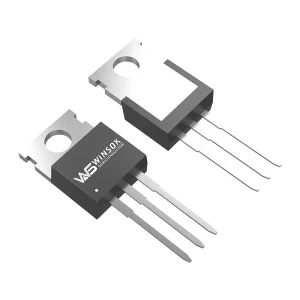
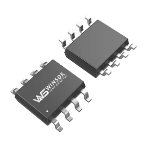
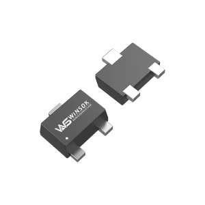
High-performance silicon components designed to lower RDS(on) and optimize thermal management in robust grid, industrial, and consumer energy storage applications.

The global transition toward decentralized renewable energy grids has positioned Battery Energy Storage Systems (BESS) at the absolute epicenter of the industrial, utility, and residential infrastructure ecosystems. At the heart of every BESS is the Battery Management System (BMS) and its corresponding Power Conversion System (PCS). These systems dictate the safety, efficiency, and operational lifespan of massive lithium-ion or sodium-ion battery architectures. In these configurations, power MOSFETs act as the primary gatekeepers of energy, managing safety-critical operations including dual-directional overcurrent protection, active and passive cell balancing, thermal runaway prevention, and high-frequency DC-DC voltage regulation.
Modern BESS architectures require semiconductors with specialized parameters. Off-the-shelf components often present compromised solutions, forcing system architects to balance higher conduction losses against reduced thermal stability. Custom-optimized MOSFETs, such as those engineered by WINSOK, address these challenges directly. By customizing parameters like gate charge ($Q_g$), turn-on resistance ($R_{DS(on)}$), and packaging parameters, engineers can achieve up to 30% reduction in thermal dissipation, directly scaling down system footprint, cooling overhead, and the Levelized Cost of Storage (LCOS).
The macro-economic landscape for global utility-scale and commercial/industrial BESS has witnessed exponential CAGR acceleration. Key trends globally illustrate distinct application profiles:
This global commercial context highlights the necessity for highly customized power semiconductors. BESS operators are shifting focus from initial capital expenditure (CAPEX) to operating expenditure (OPEX) and reliability metrics. A system failure due to MOSFET breakdown can result in severe thermal incidents or critical system downtime, underscoring the value of high-reliability components.
To design an optimized custom MOSFET for BESS, power electronics engineers must evaluate critical semiconductor parameters and target the specific trade-offs inherent in energy storage applications:
Under continuous charge/discharge cycles, conduction losses in the solid-state protection switches dominate total power dissipation. Customizing the trench gate structure allows manufacturers to drive down the specific area resistance. Winsok's proprietary Split-Gate Trench (SGT) technology allows for ultra-low $R_{DS(on)}$ configurations under 40V, 60V, and 100V platforms (e.g., WSD28N10DN33 or WSK140N03), minimizing the I²R losses that lead to thermal strain.
BESS systems face unpredictable grid transients, short circuits, and capacitive load turn-on cycles. A robust Safe Operating Area (SOA) combined with high Single-Pulse Avalanche Energy ($E_{AS}$) capacity guarantees that the MOSFET can absorb and dissipate high-energy voltage spikes without suffering gate oxide breakdown or hot-carrier degradation.
Furthermore, in parallel switching configurations typical of BMS protection boards, mismatch of threshold voltage ($V_{GS(th)}$) and parasitic inductances can result in severe current imbalance during dynamic switching states. Standard mass-market MOSFETs exhibit wider tolerances in $V_{GS(th)}$ sorting, leading to single-device thermal overload. Custom solutions require tight packaging tolerances, synchronized gate resistances ($R_g$), and matching $V_{GS(th)}$ sorting bands to ensure uniform current distribution across parallel branches.
To successfully integrate custom MOSFET products into a BESS solution, designers look at the overall system topology. The primary sub-systems leveraging customized MOSFETs include:
In high-capacity BESS packs, traditional mechanical relays are being replaced by solid-state switches due to their arc-free switching, microsecond response times, and superior cycle life. Utilizing back-to-back N-channel MOSFETs (such as the WSK140N03 or WSR25N20G) allows for bidirectional current flow blocking. Customizing the gate drive speed controls the $dV/dt$ rate during turn-on, preventing transient voltage spikes from damaging secondary sub-systems.
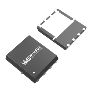
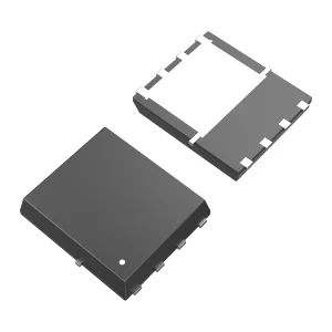
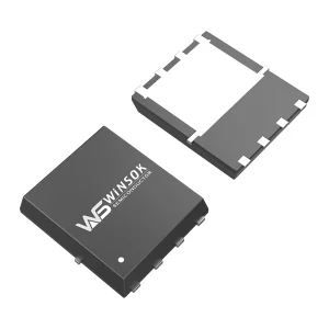
As battery packs age, individual cells diverge in State of Charge (SOC) and capacity. Active balancing topologies dynamically transfer energy from high-SOC cells to low-SOC cells using local buck-boost or flyback converter circuits. These circuits rely on miniature, fast-switching dual MOSFET configurations (e.g., the WSD4098 Dual N-Channel or WSD3067DN56 N+P-Channel) in compact DFN5X6-8L packages to maximize conversion efficiency while fitting within tight cell-monitoring module designs.


The evolution of energy storage technology continues to demand higher efficiency, density, and operating voltages. Winsok is actively working on the technological roadmap defined by several milestone vectors:
HONGKONG Olukey INDUSTRY CO., LIMITED is a comprehensive solution provider focusing on the overall integration and supply of premium electronic product components. Our core product portfolio encompasses three highly synergistic product lines: WINSOK MOSFETs, Cmsemicon MCUs, and custom PCBA circuit board solution development.
At present, the products of Olukey Industry are widely utilized across demanding domains including automotive electronics, military electronics, smart industrial applications, new energy systems, smart medical care, 5G communications, the Internet of Things (IoT), smart home applications, and consumer electronics. Relying on key advantages as global general agents of major original factories, we are based deeply in the Asia-Pacific market, providing advanced semiconductor parts through a comprehensive services model to assist global manufacturers in producing high-quality electronic solutions.
Over the years, Olukey Industry has built a strong reputation centered on the core principle of "quality first, service first." We maintain close, long-term partnerships with high-tech enterprises and original component manufacturers worldwide. By utilizing global agent resources, we secure stable supply chains, cost advantages, and provide direct technical support to our clients, assisting them from initial prototyping through to mass-production phases.




Our competitive advantage lies in active market development and resource integration within the Asia-Pacific region, making us one of the fastest-growing agents in the industry. Through our long-term partnership with WINSOK, we offer a comprehensive mid-to-low voltage MOSFET range: 15V, 20V, 30V, 40V, 60V, 80V, 100V, 120V, 150V, 200V, 250V, 300V, 400V, 500V, 600V, 650V.
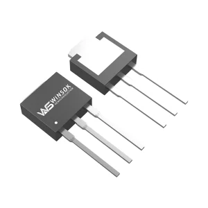
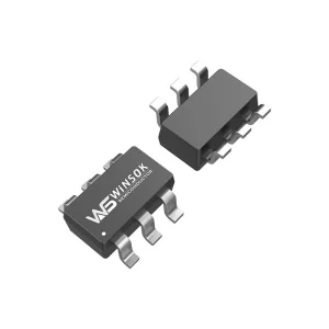
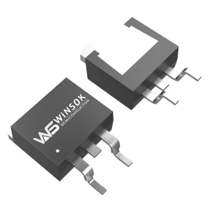
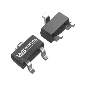
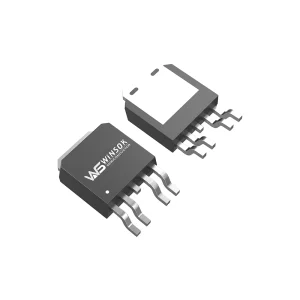
We provide these products in key industry-standard packages, including DFN3X3-8, DFN5X6-8, TO-252, TO-263, SOP-8, SOT-23, TO-220, and more. With over 600 models and 40 packages, we cover the majority of medium and low-voltage MOSFET specifications required by today's power conversion and energy storage manufacturers.
Additionally, by pairing WINSOK MOSFETs with Cmsemicon's microcontrollers (MCU), Olukey Industry offers complete, integrated solutions for battery management, motor control, and power conversion. Our team operates under the corporate values of "Pragmatism, Win-win, Service, and Responsibility," aiming to deliver reliable, high-value components that support the development and scaling of semiconductor solutions globally.

Technical insights on selecting, custom-matching, and deploying power MOSFETs within modern Battery Energy Storage Systems (BESS).
Explore our extended line of low, medium, and high-voltage MOSFETs, designed to meet diverse design requirements across industrial power and energy storage systems.

 Olukey