High-reliability engineering solutions for immediate drop-in replacement and custom electrical parameter optimization.


Decentralized Power Architectures, High-Density Demands, and the Evolution of Silicon Solid-State Switches.
Modern electrical grids, electric vehicles (EVs), cloud datacenters, and industrial automation networks demand unprecedented conversion efficiency. The historical reliance on standard legacy semiconductor components is shifting rapidly. As systems squeeze more kilowatts into smaller volumes, thermal boundaries are being pushed to their physical limits. High-frequency switched-mode power supplies (SMPS) and DC-DC converters (including buck, boost, and resonant LLC configurations) require custom-optimized MOSFETs to mitigate switching losses and parasitic oscillation. Standard off-the-shelf semiconductors often fall short in specific gate charge configurations ($Q_g$) or thermal performance parameterization.
In DC-DC converters, switching frequency directly impacts the passive component size. Increasing frequencies require MOSFETs with minimal parasitic capacitances ($C_{iss}$ and $C_{oss}$) to prevent dynamic gate-drive losses and preserve overall efficiency. Our custom MOSFET solutions enable optimized performance tailored to your design’s unique frequency parameters.
The global electronic components landscape remains highly volatile. Major original device manufacturers (ODMs) face extended lead times, legacy phase-outs, and pricing instability. For crucial power paths inside DC-DC converters, a simple supply chain delay can stall entire automotive subassembly lines or halt industrial plant installations. Custom-manufactured and strategically distributed power MOSFETs act as a vital countermeasure. By working with a reliable factory-distributor like Olukey Industry, developers secure custom silicon tailored to match or exceed the specifications of discontinued or hard-to-source international components.
Replacing a power MOSFET in a high-efficiency DC-DC converter is not merely a matter of matching package footprint and voltage breakdown limits. A comprehensive validation matrix must be scrutinized to ensure thermal stability, efficiency gains, and safe operating area (SOA) protection.
| Critical Parameter | Technical Definition | Impact on DC-DC Converter Replacement | Olukey/WINSOK Custom Capabilities |
|---|---|---|---|
| $V_{DS}$ (Breakdown Voltage) | Maximum drain-to-source voltage without avalanche breakdown. | Determines safety margin against voltage spikes during inductive switching. | 15V to 650V voltage options. |
| $R_{DS(on)}$ (On-State Resistance) | Static drain-source resistance during fully saturated conduction. | Directly dictates $I^2R$ conduction losses and thermal dissipation. | Optimized trench structures minimizing $R_{DS(on)}$ down to sub-milliohm levels. |
| $Q_g$ & $Q_{gd}$ (Gate Charge) | Charge required by the gate to turn the device fully on and off. | Impacts switching speed, gate-driver load, and cross-conduction risks. | Tailored gate charge tuning to prevent cross-talk in synchronous rectification. |
| $R_{\theta JC}$ (Thermal Resistance) | Junction-to-case thermal resistance. | Defines package power dissipation capability. | Copper-clip DFN and exposed-pad TO-packages for maximized thermal dissipation. |
Why Copper Clip Packaging, Dual Die Configuration, and Package Optimization Define the Future of Power Conversion.
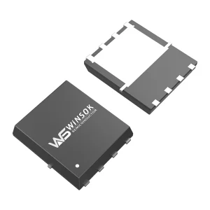
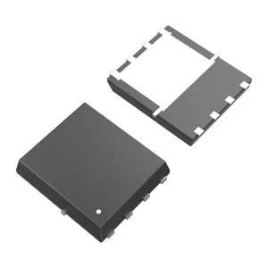
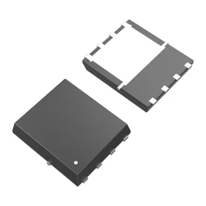
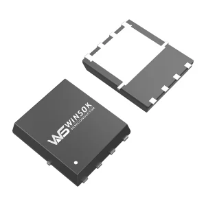
Legacy packages such as standard wire-bonded DFN and SOP designs exhibit significant parasitic package inductance. At high switching frequencies (>200 kHz), these parasitic components cause significant gate ringing, voltage spikes, and elektromagnetische Verträglichkeit (EMC) compliance issues. By deploying custom-engineered copper-clip bonding technology (as featured in our DFN3X3-8 and DFN5X6-8 MOSFET range), the internal resistance of the packaging is reduced by up to 50%, while thermal dissipation is greatly improved.
Replacing traditional wire bonds with solid copper clips reduces internal path resistance and parasitic inductance. This suppresses gate ringing and ensures cleaner switching transitions under high-load conditions.
Exposed drain pads and copper clip configurations allow heat to escape through both the motherboard and the heat sink. This reduces junction temperatures and extends component life cycles.
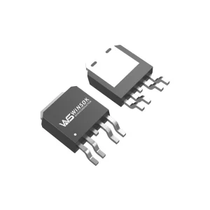
By enclosing Dual N-channel or complementary N+P channel dies inside a single DFN3X3-8 or TO-252 package, space is saved and symmetric trace layouts in synchronous buck converters are simplified.
When selecting a replacement semiconductor, engineers often encounter incompatibilities in gate-threshold voltage ($V_{GS(th)}$). A replacement MOSFET with a lower gate threshold than the original might turn on prematurely due to $dv/dt$ transients, leading to destructive cross-conduction (shoot-through). Our engineering and production facilities calibrate parameters to ensure seamless drop-in compatibility. We match key characteristics of global industry standards, including models from manufacturers like Infineon, ON Semi, and AOS (e.g., AON6572).
Hongkong Olukey Industry Co., Limited — Your Strategic Semiconductor Solution Partner.

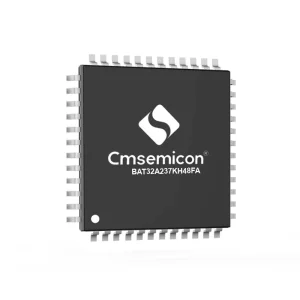
HONGKONG Olukey INDUSTRY CO., LIMITED is a leading solution provider focusing on the overall solution of electronic product components. The main products mainly include three core product lines: WINSOK MOSFET, Cmsemicon MCU, and custom PCBA circuit board solution development.
At present, the products of Olukey Industry are widely used in automotive electronics, military electronics, smart industry, new energy, smart medical care, 5G, Internet of Things, smart home, and various consumer electronics products. Relying on the advantages of global general agents of major original factories, we are based in the Asia-Pacific market. We provide customers with various advanced high-tech electronic components using comprehensive superior services, assisting manufacturers in producing high-quality products and providing comprehensive support.
Unparalleled support, extensive product catalogs, and dedicated engineering consultation.
We use comprehensive high-quality services to provide customers with various types of advanced high-tech electronic components, assist manufacturers in producing high-quality products and provide comprehensive services. Over the years, the company has relied on reputation to survive, establishing strong cooperative relationships with high-tech enterprises and original manufacturers globally.
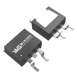
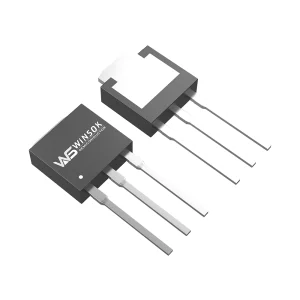
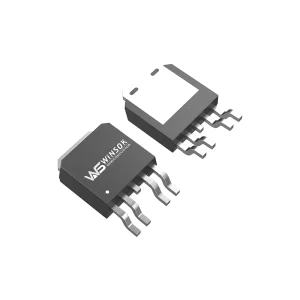
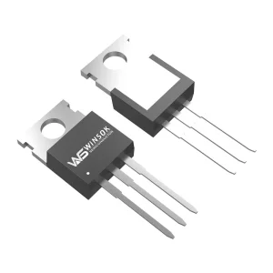
WINSOK MOSFET's product voltages are mainly medium and low voltage: 15V, 20V, 30V, 40V, 60V, 80V, 100V, 120V, 150V, 200V, 250V, 300V, 400V, 500V, 600V, 650V. The main packages include DFN3X3-8, DFN5X6-8, TO-252, TO-263, SOP-8, SOT-23, TO-220, etc. There are more than 600 models and over 40 packages, extensively covering the MOSFET product lines on the market.
Relying on the advantages of global general agents of major original manufacturers, we are based on the Asia-Pacific market. Through active market development and resource integration, we have become a fast-growing agent in the region. We work hand in hand with suppliers to explore larger markets and contribute to the semiconductor industry.






Validating Custom Components Across Automotive, Aerospace, and High-Density Digital Infrastructures.
For custom power semiconductors to gain traction in highly regulated markets, they must adhere to rigorous quality benchmarks. When replacement MOSFETs are integrated into critical systems, we ensure compliance with international testing frameworks:
A major European logistics robotics manufacturer faced long lead times for imported automotive-grade TO-252 package MOSFETs, which threatened to halt production of their Automated Guided Vehicles (AGVs). Olukey Industry analyzed the electrical schematics of the system's buck-boost DC-DC converter. By adjusting the gate-threshold voltage ($V_{GS(th)}$) to match the original driver IC's signal profile and optimizing the $R_{DS(on)}$ to reduce thermal stress, Olukey provided a custom version of the WSF40N06S N-channel 60V MOSFET. The custom replacement reduced operating temperatures by 4°C and resolved local supply delays.
Bridging the Gap Between Trench Silicon, Wide Bandgap Hybrid Systems, and Digital Control Loops.
The power electronics industry is transitioning toward Wide Bandgap (WBG) technologies, such as Gallium Nitride (GaN) and Silicon Carbide (SiC). However, standard Silicon (Si) MOSFETs remain the most cost-effective and rugged solution for low-to-medium voltage ranges (under 200V). Our technological roadmap focuses on optimizing Silicon performance while integrating smarter control systems:
By reducing pitch size on the silicon wafer, our next-generation trench gates reduce channel resistance without increasing gate capacitance, offering higher switching speeds for high-density power modules.
By leveraging Cmsemicon MCU technologies alongside custom power stages, we help developers design software-defined digital power loops. This allows real-time efficiency tuning based on dynamic thermal and load profiles.
We are tailoring the reverse recovery characteristics ($Q_{rr}$ and $t_{rr}$) of body diodes specifically for resonant LLC topologies. This minimizes recovery-current spikes and protects against high dI/dt events.
Get authoritative answers on cross-referencing, parameter calibration, and supply chain logistics for custom power MOSFETs.
Browse additional custom power designs, dual-channel configurations, and integrated microcontrollers.

 Olukey