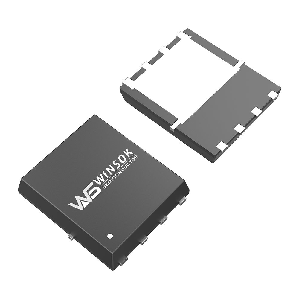
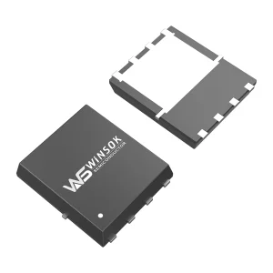
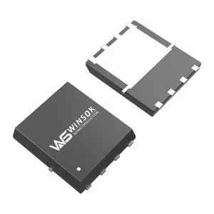
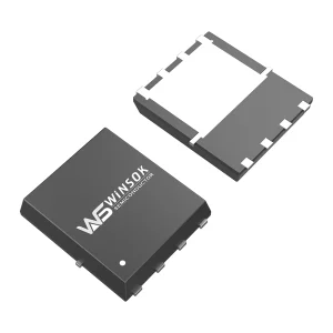
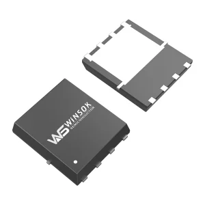
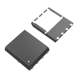
OEM WSD100N06GDN56 N-channel 60V 100A DFN5X6-8 WINSOK MOSFET Factories, Purchase

Part Number:WSD100N06GDN56 BVDSS:60V ID:100A RDSON:3mΩ   Channel:N-channel Package:DFN5X6-8

Product Description

WSD100N06GDN56 MOSFET
Voltage
60V
Current
100A
Resistance
3mΩ
Channel
N-channel
Package
DFN5X6-8
Applications
Medical power supplies MOSFET
PDs MOSFET
Drones MOSFET
Electronic cigarettes MOSFET
Major appliances MOSFET
Power tools MOSFET
Cross References
AOS MOSFET: AON6264C, AON6264E, AON6266E, AONS6662
STMicroelectronics MOSFET: STL13N6F7, STL14N6F7
PANJIT MOSFET: PSMQC33N6NS1
POTENS Semiconductor MOSFET: PDC692X
Absolute Maximum Ratings
Symbol Parameter Conditions Rating Units
VDS Drain-Source Voltage - 60 V
VGS Gate-Source Voltage - ±20 V
ID Continuous Drain Current TC=25°C 100 A
TC=100°C 65
IDM Pulsed Drain Current TC=25°C 240 A
PD Maximum Power Dissipation TC=25°C 83 W
TC=100°C 50
IAS Avalanche Current, Single pulse - 45 A
EAS Single Pulse Avalanche Energy - 101 mJ
TJ Maximum Junction Temperature - 150
TSTG Storage Temperature Range - -55 to 150
RθJA Thermal Resistance Junction to ambient Steady State 55 ℃/W
RθJC Thermal Resistance-Junction to Case Steady State 1.5 ℃/W
Electrical Characteristics
Symbol Parameter Conditions Min. Typ. Max. Unit
Static Characteristics
V(BR)DSS Drain-Source Breakdown Voltage VGS = 0V, ID = 250μA 60 - - V
IDSS Zero Gate Voltage Drain Current VDS = 48 V, VGS = 0V - - 1 µA
TJ=85°C - - 30
IGSS Gate Leakage Current VGS = ±20V, VDS = 0V - - ±100 nA
On Characteristics
VGS(TH) Gate Threshold Voltage VGS = VDS, IDS = 250µA 1.2 1.8 2.5 V
RDS(on) Drain-Source On-state Resistance VGS = 10V, ID = 20A - 3.0 3.6 mΩ
VGS = 4.5V, ID = 15A - 4.4 5.4
Switching Characteristics
Qg Total Gate Charge VDS=30V, VGS=10V, ID=20A - 58 - nC
Qgs Gate-Source Charge - 16 -
Qgd Gate-Drain Charge - 4.0 -
td(on) Turn-on Delay Time VGEN=10V, VDD=30V, ID=20A, RG=Ω - 18 - ns
tr Turn-on Rise Time - 8 -
td(off) Turn-off Delay Time - 50 -
tf Turn-off Fall Time - 11 -
Rg Gate resistance VGS=0V, VDS=0V, f=1MHz - 0.7 -
Dynamic Characteristics
Ciss Input Capacitance VGS=0V, VDS=30V, f=1MHz - 3458 - pF
Coss Output Capacitance - 1522 -
Crss Reverse Transfer Capacitance - 22 -
Drain-Source Diode Characteristics and Maximum Ratings
IS Continuous Source Current VG=VD=0V, Force Current - - 55 A
ISM Pulsed Source Current - - 240
VSD Diode Forward Voltage ISD = 1A, VGS=0V - 0.8 1.3 V
trr Reverse Recovery Time ISD=20A, dISD/dt=100A/µs - 27 - ns
Qrr Reverse Recovery Charge - 33 - nC
Frequently Asked Questions
What are the primary electrical specifications of the WSD100N06GDN56 MOSFET?
The WSD100N06GDN56 is an N-channel MOSFET featuring a drain-source breakdown voltage (VDS) of 60V, a continuous drain current (ID) of 100A, and an typical drain-source on-state resistance (RDS(on)) of 3mΩ at VGS=10V.
Which package type is the WSD100N06GDN56 MOSFET supplied in?
This device is supplied in the DFN5X6-8 package, which is ideal for high-density power layouts requiring low thermal resistance and space-saving integration.
What applications are best suited for this MOSFET?
The WSD100N06GDN56 is highly optimized for power switching applications including medical power supplies, PDs (Power Delivery), drones, electronic cigarettes, major appliances, and power tools.
Which alternative MOSFET models can cross-reference with WSD100N06GDN56?
Equivalent cross-reference options include AOS (AON6264C, AON6264E, AON6266E, AONS6662), STMicroelectronics (STL13N6F7, STL14N6F7), PANJIT (PSMQC33N6NS1), and POTENS Semiconductor (PDC692X).
What is the gate threshold voltage range (VGS(TH)) for this device?
The gate threshold voltage (VGS(TH)) of the WSD100N06GDN56 MOSFET ranges from a minimum of 1.2V to a maximum of 2.5V, with a typical value of 1.8V under test conditions of VGS = VDS and IDS = 250µA.

Related Products