Direct factory sourcing of high-performance switching devices engineered for fast charging, synchronous rectification, and load control.



In an era dominated by USB Power Delivery (USB-PD 3.0/3.1) and GaN-based topologies, selecting the ideal Silicon MOSFET is the defining factor for thermal efficiency and overall system cost optimization.
As universal chargers scale from 45W, 65W, to the latest 140W and 240W Extended Power Range (EPR) specifications, hardware developers face intense challenges. Power adapters must fit compact form factors while maintaining safe casing temperatures. Here, low drain-to-source on-resistance (RDS(on)) and minimal gate charge (Qg) are paramount.
Whether optimizing the primary-side flyback converter, implementing high-efficiency Synchronous Rectification (SR) on the secondary side, or managing safe power distribution with a VBUS load switch, specialized MOSFET topologies determine your adapter's efficiency curve. This whitepaper analyzes critical design pathways, supply chain solutions, and procurement benchmarks essential for global hardware designers and purchasing managers.

Leading the progression of semiconductor component supply networks across the Asia-Pacific region and global industrial ecosystems.

HONGKONG Olukey INDUSTRY CO., LIMITED is a comprehensive solution provider focusing on the overall integration and optimization of advanced electronic product component systems.
Our core product matrix consists of three key pillars: WINSOK MOSFETs, Cmsemicon Microcontrollers (MCUs), and custom PCBA circuit board solution development. By maintaining direct, authorized representation of top original manufacturers, Olukey provides a seamless channel for clients to acquire cutting-edge high-tech electronic components.
Our products are deployed globally across demanding sectors including automotive electronics, defense, military electronics, smart industrial environments, new energy infrastructure, intelligent medical systems, 5G wireless communications, IoT modules, and next-generation smart home systems. Backed by extensive local distribution networks and deep technical design-in expertise, we are dedicated to aiding manufacturers in streamlining production processes and improving output quality.
How semiconductor innovations are addressing the physical limits of Silicon (Si) to power the USB-PD 3.1 era.
To reach higher switching frequencies, the trade-off between RDS(on) and Qg must be minimized. Superjunction MOSFET architectures are dropping FOM thresholds, enabling rapid switching with negligible switching losses, facilitating compact transformer geometries in chargers.
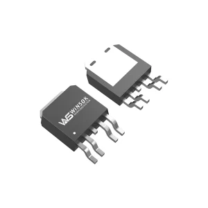
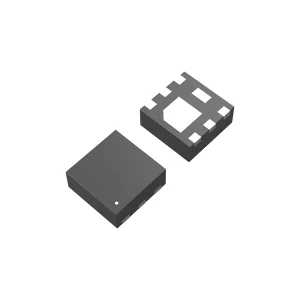
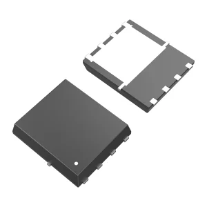
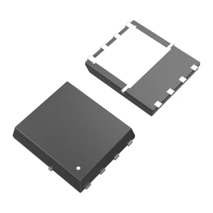
Legacy SOT and TO packages are giving way to flat leadless layouts like DFN3X3-8 and DFN5X6-8. These designs offer exceptionally low package resistance and direct thermal paths to the PCB substrate, keeping operational temperatures low under continuous load conditions.
While Gallium Nitride (GaN) handles primary switching in high-density chargers, Silicon MOSFETs remain the preferred, cost-effective standard for secondary Synchronous Rectification (SR) and VBUS port control due to their ruggedness, cost structures, and low conduction losses.
Targeted application paradigms maximizing reliability and efficiency in various commercial use-cases.
Modern chargers dynamically reallocate power to multiple USB-C ports. For instance, when a 100W charger detects two devices, it changes its topology from single 100W to dual 45W+45W or 65W+30W charging lanes. This requires robust P-channel or N-channel VBUS switches like the WST3403 or the WSD30L68DN33. Olukey integrates these switches with Cmsemicon MCUs to enable smart power negotiation (USB-PD handshake) and fast circuit-interrupt protection.
Car chargers face severe input surges and wide thermal swings. Automotive-grade buck-boost topologies rely on 40V, 60V, and 100V MOSFETs in robust TO-252 and DFN5X6-8 configurations to survive load dump pulses and keep electromagnetic emissions (EMI) below CISPR 25 standards. Our catalog, featuring the WSF80N06H and the WSF90N10, meets these challenges.
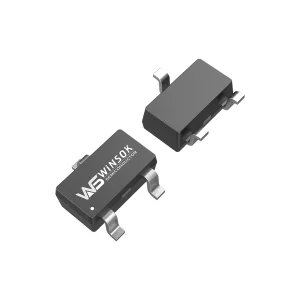
In low-power IoT networks, battery-powered and PoE devices require low-leakage power switches. Low-threshold P-channel devices (e.g., AON2409, WST3403) are crucial in reducing quiescent current during sleep modes while ensuring immediate response times upon wakeup.

Combining comprehensive, high-quality services with reliable supply chains and robust technical capabilities.

Adhering to our core philosophy of "quality first, service first," we support high-tech enterprises and manufacturers worldwide with reliable component sourcing.
Over the years, Olukey has established deep cooperative relationships with original manufacturers and packaging partners. Our engineering team provides direct design-in support, from initial schematic reviews to EMI trouble-shooting and thermal profiling, minimizing time-to-market.
We leverage our position as general agents to offer highly competitive pricing, secure supply buffers, and short lead times compared to typical broker channels. With over 600 models in more than 40 package types, our inventory covers a broad spectrum of medium- and low-voltage MOSFET specifications.
How automated packaging and smart fabrication facilities deliver high volume stability and consistent electrical performance.
Our manufacturing and assembly hubs utilize modern Factory 4.0 infrastructure to ensure high yield rates and steady batch consistency. Deep automation minimizes manual processes, resulting in an exceptionally low Defect Parts Per Million (DPPM) metric.
In a volatile global component supply chain, our strong relationships with domestic wafer foundries and automated testing facilities allow us to maintain reliable lead times and buffer stocks, shielding clients from supply disruptions.

Managing cross-reference compatibility, sourcing timelines, and package footprints for high-volume programs.

Enterprise procurement teams must balance unit costs, technical performance, and supply security. Sourcing specialized components like low-voltage N-channel and P-channel MOSFETs requires addressing several design-in considerations:
1. Pin-to-Pin Cross-Referencing: To minimize design risk, our products are engineered to be drop-in replacements for standard components from top brands. WINSOK devices (e.g., DFN5X6-8, DFN3X3-8, TO-252, SOP-8, SOT-23) offer identical or superior electrical performance compared to products from AOS, ON Semi, Toshiba, and Panjit.
2. Long-Term Reliability: Chargers run warm and face thermal fluctuations. Our parts undergo strict High-Temperature Reverse Bias (HTRB) and High-Temperature Gate Bias (HTGB) life testing, verifying parameter stability over thousands of operating hours.
3. Flexible Packaging Formats: We support both tape-and-reel (T&R) for high-speed pick-and-place lines and tube packaging for specialized manual assembly, helping manufacturers optimize their production lines.
Ensuring compliance with international safety regulations and environmental directives while offering direct technical support.
All WINSOK MOSFETs and Cmsemicon MCUs supplied by Olukey are certified for international export. Our components meet the strict standards required by major consumer markets, including RoHS and REACH compliance, ensuring lead-free and hazard-free bill-of-materials (BOM) designs.
Furthermore, our products are designed to meet safety and performance benchmarks such as UL 62368-1 for audio/video and information technology equipment, as well as CE and FCC requirements for electromagnetic compatibility. Through our localization program, we connect clients directly with local application engineers. These engineers assist with design challenges, provide custom SPICE simulation models, and offer board-level analysis to ensure your product passes certification on the first attempt.

Common design-in and sourcing questions answered by our application engineers.
DFN packages (like DFN3X3-8 and DFN5X6-8) have flat, leadless undersides. This design significantly reduces internal package resistance and parasitic inductance. They feature exposed thermal pads that contact the PCB copper planes directly, allowing heat to dissipate much faster than leaded SOP-8 packages. This enables high-current handling in compact charger enclosures.
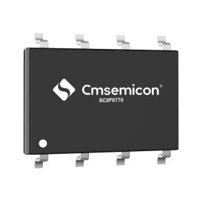
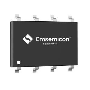
Cmsemicon MCUs (such as the SC8F6771 or CMS79FT61x) manage system-level house-keeping. They negotiate power allocation through communication protocols (like USB-PD), monitor thermal sensors, and coordinate gate drivers to turn off safety switches (VBUS MOSFETs) in case of overvoltage, overcurrent, or overtemperature faults.
For a flyback converter design, the secondary-side SR MOSFET is exposed to voltages higher than the output voltage due to transformer turns ratios and leakage inductance spikes. As a general guideline, for a 20V output design (standard USB-PD 100W), a MOSFET with a breakdown voltage rating of 80V or 100V (e.g., WSD30N10DN56T) is chosen to provide a safe operating margin.
Yes. WINSOK products are designed to cross-reference with standard parts from brands like AOS (e.g., AON2409), Onsemi (e.g., NTMFS4834N), Toshiba (e.g., TPH2R93PL), and Panjit (e.g., PJQ5476AL). Our engineering team can analyze your schematics and suggest alternative part numbers to help optimize costs or diversify your supply chain.
Browse our extended product portfolio for high-density power conversion and digital control solutions.
 Olukey