Engineered for low RDS(on), superior thermal dissipation, and industrial-grade reliability
Understanding Global Procurement Demands for Lithium-Ion Battery Protection Systems
The transition from legacy internal combustion engines and corded power systems to advanced, high-density lithium-ion (Li-ion) batteries has triggered a massive paradigm shift in power semiconductor requirements. Globally, procurement departments at major tier-one OEMs, industrial system integrators, and electric mobility suppliers face a dual challenge: shrinking physical board space and demanding higher thermal performance limits. High-performance, latest-design Power MOSFETs are critical to this evolution.
In modern Battery Management Systems (BMS), safety profiles require reliable power path interruption during overcurrent, short-circuit, and overvoltage events. The switch arrays (both N-channel and P-channel) must exhibit ultra-low drain-source on-resistance ($R_{DS(on)}$) to prevent excessive internal heating while withstanding high transient current surges. The integration of high-density battery arrays in automotive, industrial power tool, consumer electronic, and telecom backup industries has driven global demand for reliable sourcing channels, cross-reference alternatives, and engineering support structures that protect operational continuity.
Modern energy architectures demand advanced topologies that go beyond standard silicon limitations. Our primary solutions address critical pain points across multiple commercial applications:
AEC-Q101 qualified, ultra-rugged solutions configured for bidirectional protection. Able to withstand high transient currents, vibration, and extreme temperature cycling inside traction packs and auxiliary systems.
Designed for compact enclosures with low thermal resistance. Delivers sustained peak currents during high-torque operation in cordless drills, saws, and automated robotic systems.
Offers low conduction losses in scalable parallel arrays, improving round-trip efficiency in large-scale residential and containerized industrial battery installations.
By utilizing Shielded Gate Trench (SGT) architectures, our portfolio achieves a superior figure of merit ($FOM = R_{DS(on)} \times Q_g$). This optimization drastically minimizes both switching and conduction losses, allowing engineers to design thinner, lighter battery packs without risking thermal overload.
The continuous drive to scale down power electronics has pushed packaging technologies to the forefront. Traditional wire-bonded packages like the TO-220 and early DPAK variants are being phased out in high-current applications due to parasitic source wire inductance and high internal packaging resistance.
| Package Type | Thermal Resistance ($R_{\theta JC}$) | Primary Application Fields | Core Structural Advantages |
|---|---|---|---|
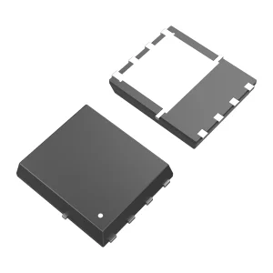
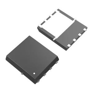
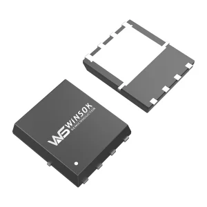
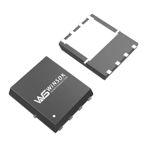
| DFN3X3-8 / DFN5X6-8 | 1.2 - 2.5 °C/W | Smartphones, laptops, portable power stations | Low profile, minimized footprint, direct-bond copper clip structure reducing parasitic inductance. |
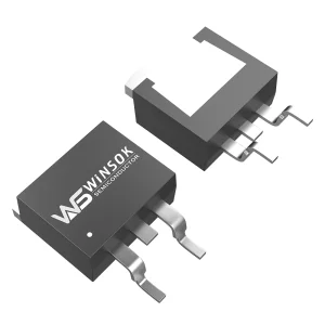
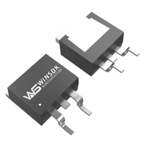
| TO-252 / TO-263-2L | 0.6 - 1.0 °C/W | Industrial motor drives, consumer power tools | Robust leads, optimized thermal path, high avalanche energy ruggedness ($E_{AS}$). |
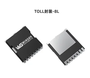
| TOLLA-8L (Toll package) | 0.4 - 0.6 °C/W | High-power BMS, e-bikes, telecommunication backup | Minimal board space compared to D2PAK, massive current handling capacity (up to 300A). |
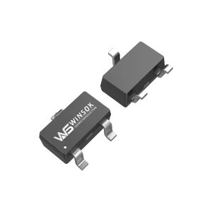
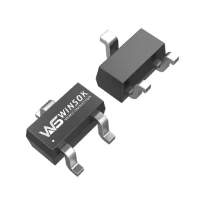
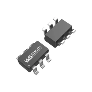
| SOT-23 / SOT-23L / SOT-523 | Typical signal load | Gate drive control circuits, auxiliary switches | Sub-miniature size, highly cost-effective, standard mounting compatibility. |
The technological roadmap focuses on transitioning low-voltage protection topologies from standard N-Channel/P-Channel layouts to advanced monolithic architectures. These designs offer features like electrostatic discharge (ESD) protection on the gate and built-in temperature sensors, improving overall reliability.
Navigating the global semiconductor supply chain requires strong quality control measures and compliance guarantees. Olukey Industry and Winsok MOSFET products are designed to meet strict international standards, ensuring seamless deployment in global markets.
We guarantee full alignment with RoHS and REACH regulations, assuring green manufacturing protocols that eliminate heavy metals and hazardous chemicals. For demanding environments, our quality management system is audited under ISO 9001 and IATF 16949 frameworks, which guarantees strict traceability from raw wafer sourcing to packaged unit testing.
Our local support infrastructure is strategically located in major electronics manufacturing hubs throughout the Asia-Pacific region, North America, and Europe. This geographic presence enables us to offer:
HONGKONG Olukey Industry Co., Limited & WINSOK MOSFET Partnership

As a leading solution provider, Olukey Industry focuses on overall component supply and electronic solution development. Our primary product portfolio consists of three key lines: WINSOK MOSFETs, Cmsemicon MCUs, and customized PCBA circuit board solutions.
At present, our products are widely integrated into automotive electronics, aerospace/military applications, industrial IoT, new energy installations, smart medical equipment, 5G communications infrastructures, and consumer electronics. Based in the Asia-Pacific market and utilizing relationships with key global semiconductor fabs, we provide advanced, high-tech electronic components with reliable, end-to-end technical support.

WINSOK MOSFET provides a comprehensive catalog of low and medium-voltage power devices. Our voltage coverage spans from 15V to 650V, encompassing over 600 distinct models in more than 40 standard packaging styles (including DFN3x3-8, DFN5x6-8, TO-252, TO-263, SOP-8, SOT-23, and TO-220).
This wide product selection makes Winsok a reliable replacement alternative for legacy and high-cost brands like Alpha & Omega Semiconductor, ON Semiconductor, Infineon, Nexperia, and Toshiba. Combined with Cmsemicon's high-efficiency MCUs, we deliver integrated, reliable system-level components.





In-depth responses from our applications engineering department
Explore our high-current and specialized voltage range MOSFET solutions
 Olukey