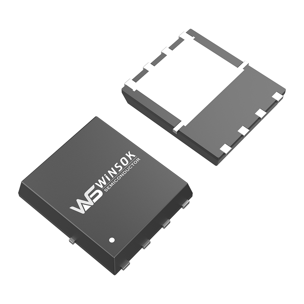
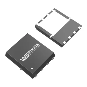
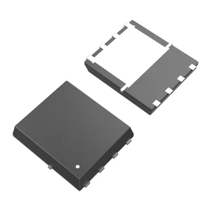
Latest design WSD40120DN56G N-channel 40V 120A DFN5X6-8 WINSOK MOSFET Factories, Distributor

Part Number:WSD40120DN56G

BVDSS:40V

ID:120A

RDSON:1.4mΩ  

Channel:N-channel

Package:DFN5X6-8

Product Description

WSD40120DN56G N-Channel MOSFET
High-performance power semiconductor designed for high efficiency switching applications.
Voltage
40V
Current
120A
Resistance
1.4mΩ
Package
DFN5X6-8
Applications
E-cigarettes MOSFET
Wireless charging MOSFET
Drones MOSFET
Medical care MOSFET
Car chargers MOSFET
Controllers MOSFET
Digital products MOSFET
Small household appliances MOSFET
Consumer electronics MOSFET
Cross Reference / Equivalents
  • AOS MOSFET AON6234, AON6232, AON623
  • STMicroelectronics MOSFET STL14N4F7AG
  • POTENS Semiconductor MOSFET PDC496X
Absolute Maximum Ratings
Symbol Parameter Rating Units
VDS Drain-Source Voltage 40 V
VGS Gate-Source Voltage ±20 V
ID @ TC=25℃ Continuous Drain Current, VGS @ 10V¹ 120 A
ID @ TC=100℃ Continuous Drain Current, VGS @ 10V¹ 82 A
IDM Pulsed Drain Current² 400 A
EAS Single Pulse Avalanche Energy³ 400 mJ
IAS Avalanche Current 40 A
PD @ TC=25℃ Total Power Dissipation⁴ 125 W
TSTG Storage Temperature Range -55 to 150
TJ Operating Junction Temperature Range -55 to 150
Electrical Characteristics
Symbol Parameter Conditions Min. Typ. Max. Unit
BVDSS Drain-Source Breakdown Voltage VGS=0V, ID=250uA 40 --- --- V
△BVDSS/△TJ BVDSS Temperature Coefficient Reference to 25℃, ID=1mA --- 0.043 --- V/℃
RDS(ON) Static Drain-Source On-Resistance² VGS=10V, ID=20A --- 1.4 1.8
RDS(ON) Static Drain-Source On-Resistance² VGS=4.5V, ID=20A --- 2.0 2.6
VGS(th) Gate Threshold Voltage VGS=VDS, ID=250uA 1.2 1.6 2.2 V
△VGS(th) VGS(th) Temperature Coefficient --- -6.94 --- mV/℃
IDSS Drain-Source Leakage Current VDS=32V, VGS=0V, TJ=25℃ --- --- 1 uA
VDS=32V, VGS=0V, TJ=55℃ --- --- 5
IGSS Gate-Source Leakage Current VGS=±20V, VDS=0V --- --- ±100 nA
gfs Forward Transconductance VDS=5V, ID=20A --- 53 --- S
Rg Gate Resistance VDS=0V, VGS=0V, f=1MHz --- 1.0 --- Ω
Qg Total Gate Charge (10V) VDS=15V, VGS=10V, ID=20A --- 45 --- nC
Qgs Gate-Source Charge --- 12 ---
Qgd Gate-Drain Charge --- 18.5 ---
Td(on) Turn-On Delay Time VDD=15V, VGEN=10V, RG=3.3 Ω, ID=20A, RL=15Ω --- 18.5 --- ns
Tr Rise Time --- 9 ---
Td(off) Turn-Off Delay Time --- 58.5 ---
Tf Fall Time --- 32 ---
Ciss Input Capacitance VDS=20V, VGS=0V, f=1MHz --- 3972 --- pF
Coss Output Capacitance --- 1119 ---
Crss Reverse Transfer Capacitance --- 82 ---
Frequently Asked Questions
What are the primary specifications of the WSD40120DN56G MOSFET?
The WSD40120DN56G is an N-channel MOSFET featuring a drain-source voltage (VDS) of 40V, continuous drain current (ID) of 120A, and a static drain-source on-resistance (RDS(ON)) of 1.4mΩ, packaged in a compact DFN5X6-8 package.
Which devices and applications are compatible with this MOSFET?
It is highly suitable for electronic cigarettes, wireless charging systems, drone power boards, medical devices, car chargers, controllers, digital products, small household appliances, and other consumer electronics.
What is the thermal operating range of the WSD40120DN56G?
This MOSFET has a rated operating junction temperature (TJ) and storage temperature range of -55 to 150℃, ensuring reliable performance in both low and high-temperature environments.
Are there cross-reference equivalents available for this MOSFET?
Yes, equivalent options that share compatible configurations include AOS models (AON6234, AON6232, AON623), STMicroelectronics (STL14N4F7AG), and POTENS Semiconductor (PDC496X).
What is the typical gate threshold voltage for the WSD40120DN56G?
The gate threshold voltage (VGS(th)) typically operates at 1.6V, with a minimum threshold limit of 1.2V and a maximum limit of 2.2V under a 250uA drain current condition.
What is the total power dissipation capability?
The WSD40120DN56G MOSFET supports a total maximum power dissipation (PD) of 125W when operating at a case temperature (TC) of 25℃.

Related Products