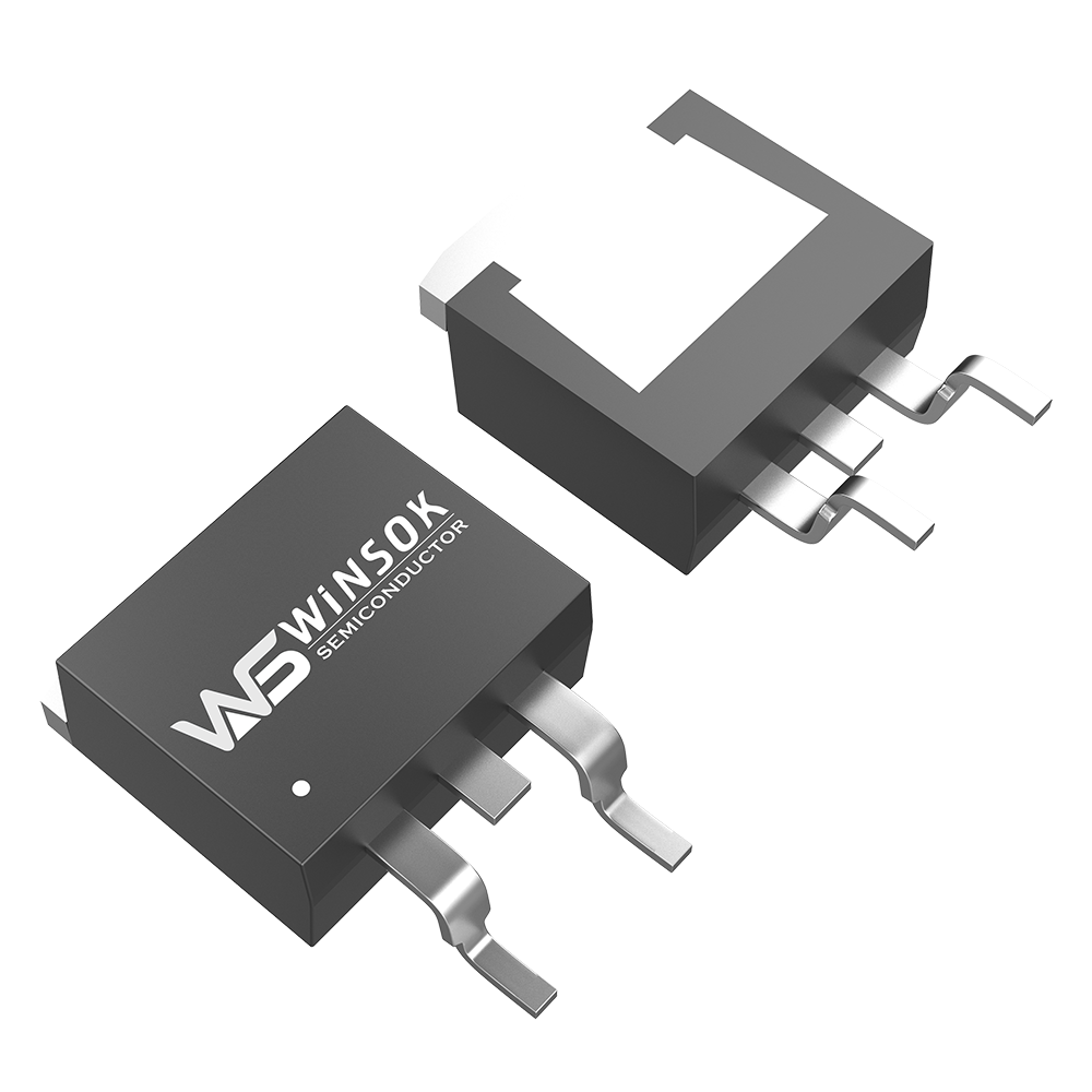
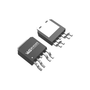
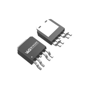
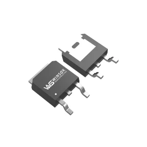
The WSK35N25 is a high-performance N-channel MOSFET designed for efficient power management and switching applications. With outstanding voltage and current handling, it provides reliable performance in a compact TO-263-2L package.
Voltage (VDS)
250V
Current (ID)
35A
Resistance (RDS(on))
100mΩ
Package
TO-263-2L
Applications
E-cigaretteWireless chargerMotorEmergency power supplyDroneMedicalCar chargerController3D printerDigital productsSmall appliancesConsumer electronics
Technical Specifications
Part Number
Configuration
Type
VDS
VGS
ID (A)
RDS(ON) (mΩ)
RDS(ON) (mΩ)
Ciss
Package
@10V
@6V
@4.5V
@2.5V
@1.8V
(V)
±(V)
Max.
Typ.
Max.
Typ.
Max.
Typ.
Max.
Typ.
Max.
Typ.
(pF)
WSK35N25
Single
N-Ch
250
30
35
100
130
-
-
-
-
-
-
-
-
1969
TO-263-2L
Frequently Asked Questions
What is the voltage and current rating of the WSK35N25 MOSFET?
The WSK35N25 MOSFET has a drain-to-source voltage (VDS) of 250V and a continuous drain current (ID) rating of 35A.
What is the channel type and configuration of this semiconductor device?
The WSK35N25 is configured as a Single N-channel (N-Ch) MOSFET.
What is the on-state resistance (RDS(on)) of the WSK35N25?
At a gate-to-source voltage (VGS) of 10V, the typical RDS(on) is 130mΩ, with a maximum resistance of 100mΩ.
Which package type is used for WSK35N25?
This MOSFET is housed in a standard TO-263-2L package, which offers efficient thermal performance and standard surface mount capability.
What are the typical applications for this MOSFET?
It is commonly applied in E-cigarettes, wireless chargers, motors, emergency power supplies, drones, medical devices, car chargers, controllers, 3D printers, digital products, small appliances, and consumer electronics.
What is the input capacitance (Ciss) of the WSK35N25?
The input capacitance (Ciss) is rated at 1969 pF, helping to support fast switching speeds.
 Olukey