Olukey
1 / 1
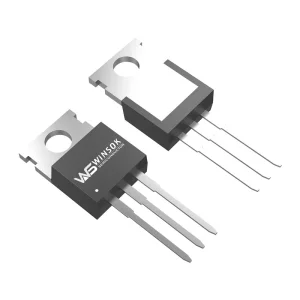
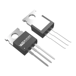
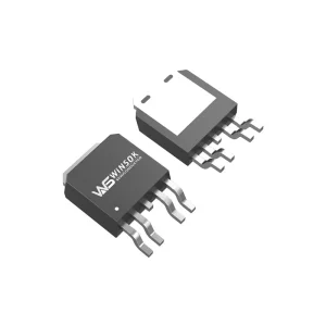
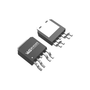
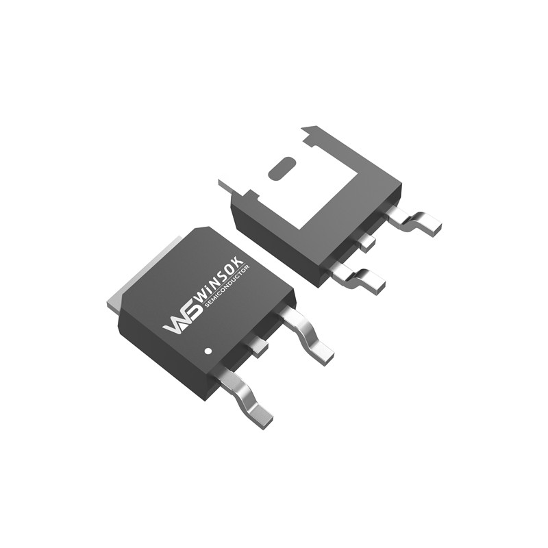
The WSF70P02 MOSFET is a top-performing P-channel trench device designed with high cell density. It delivers outstanding RDS(ON) and gate charge characteristics, making it highly efficient for most synchronous buck converter applications.
This reliable device meets all RoHS and Green Product requirements, guarantees 100% EAS, and has been approved for full function reliability.
Advanced Trench Technology with high cell density
Super low gate charge performance
Excellent reduction in CdV/dt effect
100% EAS Guaranteed for ruggedness
Environmentally-friendly device options
| Symbol | Parameter | Rating | Units | |
| 10s | Steady State | |||
| VDS | Drain-Source Voltage | -20 | V | |
| VGS | Gate-Source Voltage | ±12 | V | |
| ID @TC=25℃ | Continuous Drain Current, VGS @ -10V | -70 | A | |
| ID @TC=100℃ | Continuous Drain Current, VGS @ -10V | -36 | A | |
| IDM | Pulsed Drain Current | -200 | A | |
| EAS | Single Pulse Avalanche Energy | 360 | mJ | |
| IAS | Avalanche Current | -55.4 | A | |
| PD @TC=25℃ | Total Power Dissipation | 80 | W | |
| TSTG | Storage Temperature Range | -55 to 150 | ℃ | |
| TJ | Operating Junction Temperature Range | -55 to 150 | ℃ | |
| Symbol | Parameter | Conditions | Min. | Typ. | Max. | Unit |
| BVDSS | Drain-Source Breakdown Voltage | VGS=0V , ID=-250uA | -20 | --- | --- | V |
| △BVDSS/△TJ | BVDSS Temperature Coefficient | Reference to 25℃ , ID=-1mA | --- | -0.018 | --- | V/℃ |
| RDS(ON) | Static Drain-Source On-Resistance | VGS=-4.5V , ID=-15A | --- | 6.8 | 9.0 | mΩ |
| VGS=-2.5V , ID=-10A | --- | 8.2 | 11 | |||
| VGS(th) | Gate Threshold Voltage | VGS=VDS , ID =-250uA | -0.4 | -0.6 | -1.2 | V |
| △VGS(th) | VGS(th) Temperature Coefficient | --- | --- | 2.94 | --- | mV/℃ |
| IDSS | Drain-Source Leakage Current | VDS=-20V , VGS=0V , TJ=25℃ | --- | --- | 1 | uA |
| VDS=-20V , VGS=0V , TJ=55℃ | --- | --- | 5 | |||
| IGSS | Gate-Source Leakage Current | VGS=±12V , VDS=0V | --- | --- | ±100 | nA |
| gfs | Forward Transconductance | VDS=-5V , ID=-10A | --- | 45 | --- | S |
| Qg | Total Gate Charge (-4.5V) | VDS=-15V , VGS=-4.5V , ID=-10A | --- | 63 | --- | nC |
| Qgs | Gate-Source Charge | --- | 9.1 | --- | ||
| Qgd | Gate-Drain Charge | --- | 13 | --- | ||
| Td(on) | Turn-On Delay Time | VDD=-10V , VGS=-4.5V , RG=3.3Ω, ID=-10A | --- | 16 | --- | ns |
| Tr | Rise Time | --- | 77 | --- | ||
| Td(off) | Turn-Off Delay Time | --- | 195 | --- | ||
| Tf | Fall Time | --- | 186 | --- | ||
| Ciss | Input Capacitance | VDS=-10V , VGS=0V , f=1MHz | --- | 5783 | --- | pF |
| Coss | Output Capacitance | --- | 520 | --- | ||
| Crss | Reverse Transfer Capacitance | --- | 445 | --- |
The WSF70P02 is a high-performance P-channel MOSFET developed using advanced trench technology, featuring high cell density for minimized conduction losses.
The WSF70P02 has a maximum Drain-Source Voltage (VDS) of -20V and a continuous Drain Current (ID) rating of -70A at a case temperature of 25℃.
The typical Static Drain-Source On-Resistance is 6.8 mΩ at a Gate-Source Voltage (VGS) of -4.5V, and 8.2 mΩ at a VGS of -2.5V.
Yes, the device fully meets both RoHS and Green Product requirements, with options available for completely environmentally-friendly applications.
The WSF70P02 is 100% EAS (Single Pulse Avalanche Energy) guaranteed with a rating of 360mJ, ensuring ruggedness and reliability under extreme operating conditions.