Olukey
1 / 1
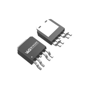
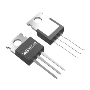
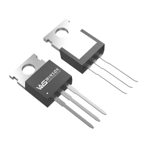
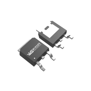
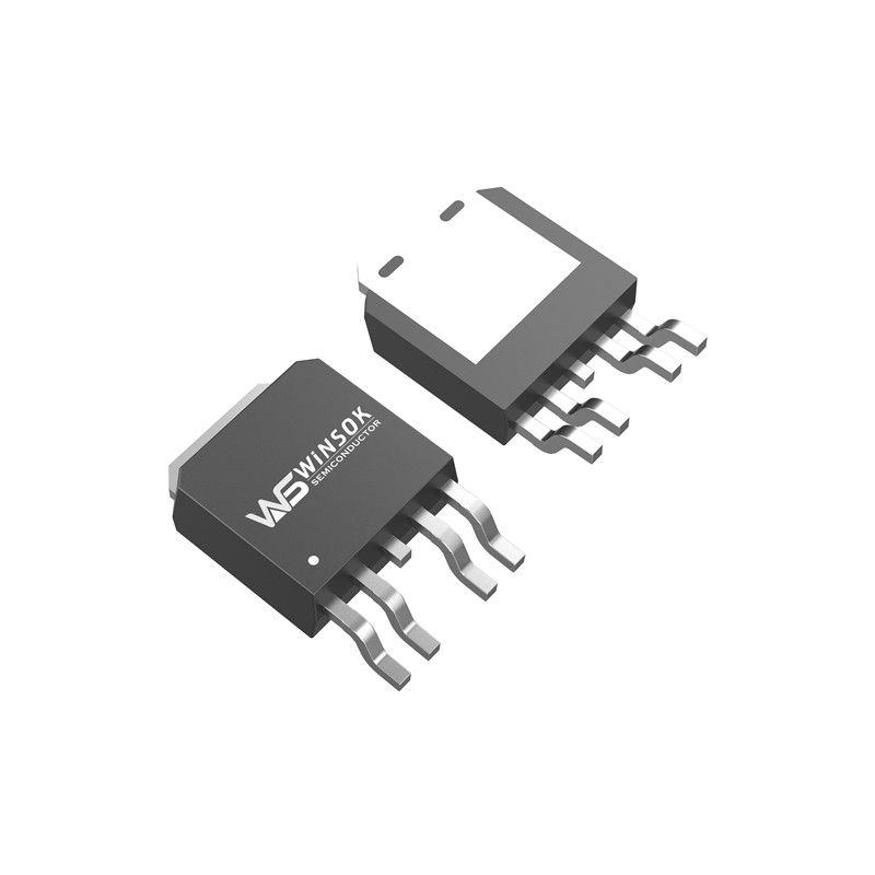
The WSF4022 is the highest performance trench Dual N-Ch MOSFET with extreme high cell density, which provide excellent RDSON and gate charge for most of the synchronous buck converter applications. The WSF4022 meets the RoHS and Green Product requirement with 100% EAS guaranteed and full function reliability approved.
| Symbol | Parameter | Condition | Rating | Units |
|---|---|---|---|---|
| VDS | Drain-Source Voltage | 40 | V | |
| VGS | Gate-Source Voltage | ±20 | V | |
| ID | Drain Current (Continuous) *AC | TC=25°C | 20* | A |
| ID | Drain Current (Continuous) *AC | TC=100°C | 20* | A |
| ID | Drain Current (Continuous) *AC | TA=25°C | 12.2 | A |
| ID | Drain Current (Continuous) *AC | TA=70°C | 10.2 | A |
| IDMa | Pulsed Drain Current | TC=25°C | 80* | A |
| EASb | Single Pulse Avalanche Energy | L=0.5mH | 25 | mJ |
| IAS b | Avalanche Current | L=0.5mH | 17.8 | A |
| PD | Maximum Power Dissipation | TC=25°C | 39.4 | W |
| PD | Maximum Power Dissipation | TC=100°C | 19.7 | W |
| PD | Power Dissipation | TA=25°C | 6.4 | W |
| PD | Power Dissipation | TA=70°C | 4.2 | W |
| TJ | Operating Junction Temperature Range | 175 | ℃ | |
| TSTG | Operating Temperature/ Storage Temperature | -55~175 | ℃ | |
| RθJA b | Thermal Resistance Junction-Ambient | Steady State c | 60 | ℃/W |
| RθJC | Thermal Resistance Junction to Case | 3.8 | ℃/W |
| Symbol | Parameter | Conditions | Min. | Typ. | Max. | Unit |
|---|---|---|---|---|---|---|
| Static Parameters | ||||||
| V(BR)DSS | Drain-Source Breakdown Voltage | VGS = 0V, ID = 250μA | 40 | V | ||
| IDSS | Zero Gate Voltage Drain Current | VDS = 32V, VGS = 0V | 1 | µA | ||
| IDSS | Zero Gate Voltage Drain Current | VDS = 32V, VGS = 0V, TJ=85°C | 30 | µA | ||
| IGSS | Gate Leakage Current | VGS = ±20V, VDS = 0V | ±100 | nA | ||
| VGS(th) | Gate Threshold Voltage | VGS = VDS, IDS = 250µA | 1.1 | 1.6 | 2.5 | V |
| RDS(on) d | Drain-Source On-state Resistance | VGS = 10V, ID = 10A | 16 | 21 | mΩ | |
| VGS = 4.5V, ID = 5A | 18 | 25 | mΩ | |||
| Gate Charge Parameters | ||||||
| Qg | Total Gate Charge | VDS=20V, VGS=4.5V, ID=10A | 7.5 | nC | ||
| Qgs | Gate-Source Charge | 3.24 | nC | |||
| Qgd | Gate-Drain Charge | 2.75 | nC | |||
| Dynamic Parameters | ||||||
| Ciss | Input Capacitance | VGS=0V, VDS=20V, f=1MHz | 815 | pF | ||
| Coss | Output Capacitance | 95 | pF | |||
| Crss | Reverse Transfer Capacitance | 60 | pF | |||
| td (on) | Turn-on Delay Time | VDD=20V, VGEN=10V, IDS=1A, RG=6Ω, RL=20Ω | 7.8 | ns | ||
| tr | Turn-on Rise Time | 6.9 | ns | |||
| td(off) | Turn-off Delay Time | 22.4 | ns | |||
| tf | Turn-off Fall Time | 4.8 | ns | |||
| Diode Parameters | ||||||
| VSDd | Diode Forward Voltage | ISD=1A, VGS=0V | 0.75 | 1.1 | V | |
| trr | Reverse Recovery Time (Input Capacitance) | IDS=10A, dlSD/dt=100A/µs | 13 | ns | ||
| Qrr | Reverse Recovery Charge (Output Capacitance) | 8.7 | nC | |||