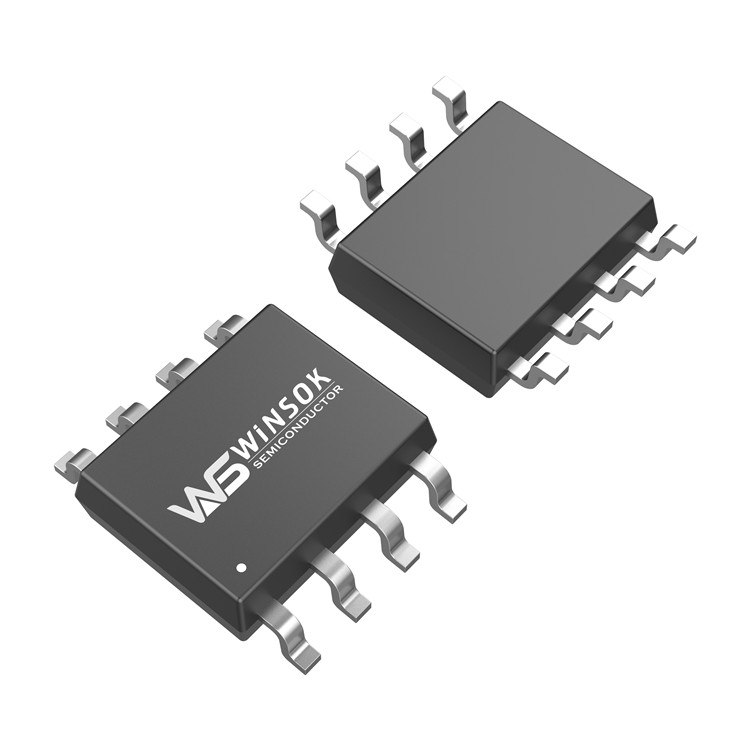
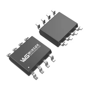
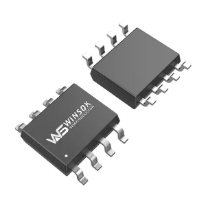
The WSP4088 is the highest performance trench N-channel MOSFET with very high cell density, providing excellent RDS(ON) and gate charge for most synchronous buck converter applications. WSP4088 complies with RoHS and green product requirements, 100% EAS guarantee, and full function reliability approved.
Key Features
Reliable and Rugged, Lead Free and Green Devices Available.
Cross-References
AO AO4884AO4882ON FDS4672APANJIT PJL9424DINTEK DTM4916
Absolute Maximum Ratings
Symbol
Parameter
Conditions
Rating
Unit
Common Ratings
VDSS
Drain-Source Voltage
-
40
V
VGSS
Gate-Source Voltage
-
±20
TJ
Maximum Junction Temperature
-
150
°C
TSTG
Storage Temperature Range
-
-55 to 150
IS
Diode Continuous Forward Current
TA=25°C
2
A
ID
Continuous Drain Current
TA=25°C
11
A
TA=70°C
8.4
IDMa
Pulsed Drain Current
TA=25°C
30
PD
Maximum Power Dissipation
TA=25°C
2.08
W
TA=70°C
1.3
RqJA
Thermal Resistance-Junction to Ambient
t ≤ 10s
30
°C/W
Steady State
60
RqJL
Thermal Resistance-Junction to Lead
Steady State
20
IASb
Avalanche Current, Single pulse
L=0.1mH
23
A
EASb
Avalanche Energy, Single pulse
L=0.1mH
26
mJ
Electrical Characteristics
Symbol
Parameter
Test Conditions
Min.
Typ.
Max.
Unit
Static Characteristics
BVDSS
Drain-Source Breakdown Voltage
VGS=0V, IDS=250μA
40
-
-
V
IDSS
Zero Gate Voltage Drain Current
VDS=32V, VGS=0V
-
-
1
μA
VDS=32V, VGS=0V, TJ=85°C
-
-
30
VGS(th)
Gate Threshold Voltage
VDS=VGS, IDS=250μA
1.5
1.8
2.5
V
IGSS
Gate Leakage Current
VGS=±20V, VDS=0V
-
-
±100
nA
RDS(ON)c
Drain-Source On-state Resistance
VGS=10V, IDS=7A
-
10.5
13
mΩ
VGS=10V, IDS=7A, TJ=125°C
-
15.75
-
VGS=4.5V, IDS=5A
-
12
16
Gfs
Forward Transconductance
VDS=5V, IDS=15A
-
31
-
S
Diode Characteristics
VSDc
Diode Forward Voltage
ISD=10A, VGS=0V
-
0.9
1.1
V
trr
Reverse Recovery Time
VDD=20V, ISD=10A, dISD/dt=100A/μs
-
15.2
-
ns
ta
Charge Time
-
9.4
-
tb
Discharge Time
-
5.8
-
Qrr
Reverse Recovery Charge
-
9.5
-
nC
Dynamic Characteristicsd
RG
Gate Resistance
VGS=0V, VDS=0V, F=1MHz
0.7
1.1
1.8
Ω
Ciss
Input Capacitance
VGS=0V, VDS=20V, Frequency=1.0MHz
-
1125
-
pF
Coss
Output Capacitance
-
132
-
Crss
Reverse Transfer Capacitance
-
70
-
td(ON)
Turn-on Delay Time
VDD=20V, RL=20Ω, IDS=1A, VGEN=10V, RG=1Ω
-
12.6
-
ns
tr
Turn-on Rise Time
-
10
-
td(OFF)
Turn-off Delay Time
-
23.6
-
tf
Turn-off Fall Time
-
6
-
Gate Charge Characteristicsd
Qg
Total Gate Charge
VDS=20V, VGS=4.5V, IDS=7A
-
9.4
-
nC
Qg
Total Gate Charge
VDS=20V, VGS=10V, IDS=7A
-
20
28
Qgth
Threshold Gate Charge
-
2
-
Qgs
Gate-Source Charge
-
3.9
-
Qgd
Gate-Drain Charge
-
3
-
Applications
Power & Computing
Power Management in Desktop Computers, DC/DC Converters, Wireless Charging.
Consumer Electronics
Electronic cigarettes, Digital products, Small household appliances, Drones.
Industrial & Automotive
Motors, Medical equipment, Car charging, Controllers.
Technical Notes:
Note a: Max. current is limited by bonding wire. Note b: UIS tested and pulse width limited by maximum junction temperature 150°C (initial temperature Tj=25°C). Note c: Pulse test; pulse width ≤ 300μs, duty cycle ≤ 2%.
Frequently Asked Questions (FAQ)
What type of MOSFET is the WSP4088?
The WSP4088 is a high-performance trench N-channel MOSFET designed with very high cell density to offer excellent low on-resistance (RDS(ON)) and low gate charge.
What are the primary applications for the WSP4088 MOSFET?
It is primarily used in desktop computer power management, DC/DC converters, wireless charging, electronic cigarettes, motors, drones, medical systems, car chargers, and smart controllers.
What is the Drain-Source Voltage (VDSS) rating of this device?
The WSP4088 has a rated maximum Drain-Source Voltage (VDSS) of 40V, making it suitable for low-to-medium voltage synchronous buck converters.
Is the WSP4088 compliant with environmental standards?
Yes. The WSP4088 fully complies with RoHS guidelines and green product requirements, utilizing lead-free manufacturing processes.
What devices can be cross-referenced or replaced by WSP4088?
Common cross-reference options include AO AO4884, AO4882, ON Semiconductor FDS4672A, PANJIT PJL9424, and DINTEK DTM4916.
What is the thermal operating range of the WSP4088?
The maximum junction operating temperature (TJ) is 150°C, with a storage temperature range (TSTG) spanning from -55°C to 150°C.
 Olukey