Olukey
1 / 1
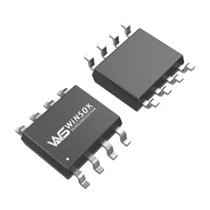
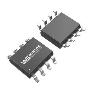
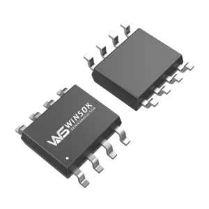
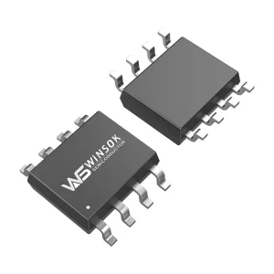
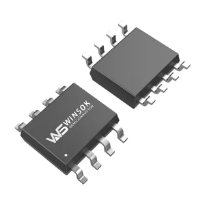
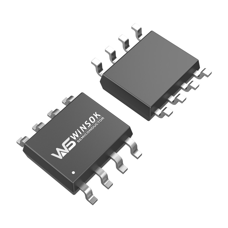
The WSP4888 is a high-performing transistor with a dense cell structure, ideal for use in synchronous buck converters. It boasts excellent RDSON and gate charges, making it a top choice for these applications. Additionally, the WSP4888 meets both RoHS and Green Product requirements and comes with a 100% EAS guarantee for reliable function.
Features high cell density and super low gate charge, significantly reducing the CdV/dt effect. Devices come with a 100% EAS guarantee and environmentally friendly options.
Each unit is thoroughly tested for performance, durability, and reliability, ensuring a long product life. Rugged design enables it to withstand extreme working conditions.
Despite superior quality, these MOSFETs are highly competitively priced, providing significant cost savings without compromising performance.
Compatible with a variety of electronic systems. Integrates seamlessly into existing designs, enhancing overall performance without major modifications.
This device can be used in place of or as an equivalent to the following industry models:
| Symbol | Parameter | Rating | Units |
|---|---|---|---|
| VDS | Drain-Source Voltage | 30 | V |
| VGS | Gate-Source Voltage | ±20 | V |
| ID@TC=25℃ | Continuous Drain Current, VGS @ 10V1 | 9.8 | A |
| ID@TC=70℃ | Continuous Drain Current, VGS @ 10V1 | 8.0 | A |
| IDM | Pulsed Drain Current2 | 45 | A |
| EAS | Single Pulse Avalanche Energy3 | 25 | mJ |
| IAS | Avalanche Current | 12 | A |
| PD@TA=25℃ | Total Power Dissipation4 | 2.0 | W |
| TSTG | Storage Temperature Range | -55 to 150 | ℃ |
| TJ | Operating Junction Temperature Range | -55 to 150 | ℃ |
| Symbol | Parameter | Conditions | Min. | Typ. | Max. | Unit |
|---|---|---|---|---|---|---|
| BVDSS | Drain-Source Breakdown Voltage | VGS=0V , ID=250uA | 30 | --- | --- | V |
| △BVDSS/△TJ | BVDSS Temperature Coefficient | Reference to 25℃ , ID=1mA | --- | 0.034 | --- | V/℃ |
| RDS(ON) | Static Drain-Source On-Resistance2 | VGS=10V , ID=8.5A | --- | 13.5 | 18 | mΩ |
| VGS=4.5V , ID=5A | --- | 18 | 25 | |||
| VGS(th) | Gate Threshold Voltage | VGS=VDS , ID =250uA | 1.5 | 1.8 | 2.5 | V |
| △VGS(th) | VGS(th) Temperature Coefficient | VGS=VDS , ID =250uA | --- | -5.8 | --- | mV/℃ |
| IDSS | Drain-Source Leakage Current | VDS=24V , VGS=0V , TJ=25℃ | --- | --- | 1 | uA |
| VDS=24V , VGS=0V , TJ=55℃ | --- | --- | 5 | |||
| IGSS | Gate-Source Leakage Current | VGS=±20V , VDS=0V | --- | --- | ±100 | nA |
| gfs | Forward Transconductance | VDS=5V , ID=8A | --- | 9 | --- | S |
| Rg | Gate Resistance | VDS=0V , VGS=0V , f=1MHz | --- | 1.8 | 2.9 | Ω |
| Qg | Total Gate Charge (4.5V) | VDS=15V , VGS=4.5V , ID=8.8A | --- | 6 | 8.4 | nC |
| Qgs | Gate-Source Charge | --- | 1.5 | --- | ||
| Qgd | Gate-Drain Charge | --- | 2.5 | --- | ||
| Td(on) | Turn-On Delay Time | VDD=15V , VGEN=10V , RG=6Ω, ID=1A, RL=15Ω | --- | 7.5 | 9.8 | ns |
| Tr | Rise Time | --- | 9.2 | 19 | ||
| Td(off) | Turn-Off Delay Time | --- | 19 | 34 | ||
| Tf | Fall Time | --- | 4.2 | 8 | ||
| Ciss | Input Capacitance | VDS=15V , VGS=0V , f=1MHz | --- | 590 | 701 | pF |
| Coss | Output Capacitance | --- | 98 | 112 | ||
| Crss | Reverse Transfer Capacitance | --- | 59 | 91 |
High Frequency Point-of-Load Synchronous Buck Converter designed for use in:
The WSP4888 is a high-performing MOSFET designed with a dense cell structure. It is optimized primarily for high-frequency point-of-load synchronous buck converters across various digital and power systems.
The transistor features Advanced Trench Technology, which yields high cell density and a super low gate charge. This combination significantly reduces the CdV/dt effect, providing excellent RDSON performance.
Yes, the WSP4888 meets both RoHS and Green Product environmental requirements, making it suitable for modern eco-friendly designs.
Every device comes with a 100% Single Pulse Avalanche Energy (EAS) guarantee, rated at 25mJ, and has undergone strict quality control and testing for long-term reliability and durability under demanding loads.
The WSP4888 is compatible with and can replace several industry standards, including AOS (AO4832, AO4838, AO4914), ON (NTMS4916N), VISHAY (Si4128DY), INFINEON (BSO150N03MD G), Sinopower (SM4803DSK), dintek (DTM4926, DTM4936), and ruichips (RU30D10H).
The WSP4888 supports a maximum Drain-Source Voltage (VDS) of 30V, a Gate-Source Voltage (VGS) of ±20V, and a continuous drain current (ID) of up to 9.8A at TC=25℃.