Olukey
1 / 1
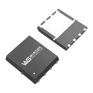
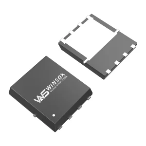
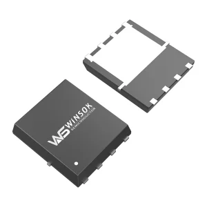
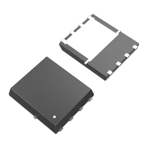
WSD40120DN56G MOSFET Specification:
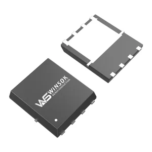
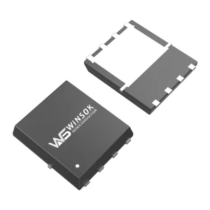
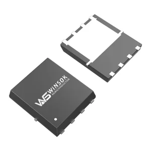
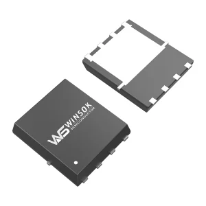
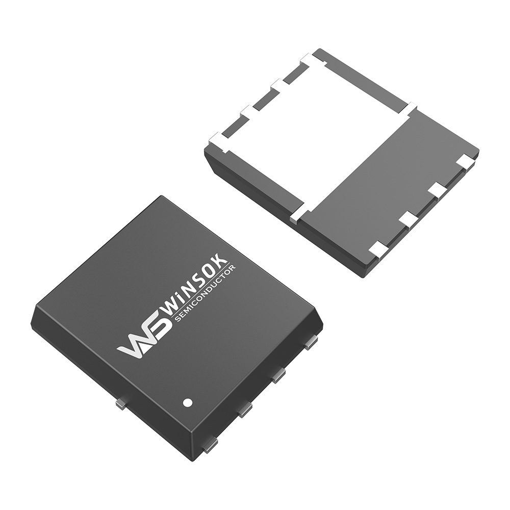
Voltage: 40V | Current: 120A | Resistance: 1.4mΩ | Channel: N-channel | Package: DFN5X6-8
| Symbol | Parameter | Rating | Units |
|---|---|---|---|
| VDS | Drain-Source Voltage | 40 | V |
| VGS | Gate-Source Voltage | ±20 | V |
| ID @ TC=25℃ | Continuous Drain Current, VGS @ 10V1 | 120 | A |
| ID @ TC=100℃ | Continuous Drain Current, VGS @ 10V1 | 82 | A |
| IDM | Pulsed Drain Current2 | 400 | A |
| EAS | Single Pulse Avalanche Energy3 | 400 | mJ |
| IAS | Avalanche Current | 40 | A |
| PD @ TC=25℃ | Total Power Dissipation4 | 125 | W |
| TSTG | Storage Temperature Range | -55 to 150 | ℃ |
| TJ | Operating Junction Temperature Range | -55 to 150 | ℃ |
| Symbol | Parameter | Conditions | Min. | Typ. | Max. | Unit |
|---|---|---|---|---|---|---|
| BVDSS | Drain-Source Breakdown Voltage | VGS=0V, ID=250uA | 40 | --- | --- | V |
| △BVDSS/△TJ | BVDSS Temperature Coefficient | Reference to 25℃, ID=1mA | --- | 0.043 | --- | V/℃ |
| RDS(ON) | Static Drain-Source On-Resistance2 | VGS=10V, ID=20A | --- | 1.4 | 1.8 | mΩ |
| RDS(ON) | Static Drain-Source On-Resistance2 | VGS=4.5V, ID=20A | --- | 2.0 | 2.6 | mΩ |
| VGS(th) | Gate Threshold Voltage | VGS=VDS, ID=250uA | 1.2 | 1.6 | 2.2 | V |
| △VGS(th) | VGS(th) Temperature Coefficient | --- | -6.94 | --- | mV/℃ | |
| IDSS | Drain-Source Leakage Current | VDS=32V, VGS=0V, TJ=25℃ | --- | --- | 1 | uA |
| VDS=32V, VGS=0V, TJ=55℃ | --- | --- | 5 | |||
| IGSS | Gate-Source Leakage Current | VGS=±20V, VDS=0V | --- | --- | ±100 | nA |
| gfs | Forward Transconductance | VDS=5V, ID=20A | --- | 53 | --- | S |
| Rg | Gate Resistance | VDS=0V, VGS=0V, f=1MHz | --- | 1.0 | --- | Ω |
| Qg | Total Gate Charge (10V) | VDS=15V, VGS=10V, ID=20A | --- | 45 | --- | nC |
| Qgs | Gate-Source Charge | --- | 12 | --- | ||
| Qgd | Gate-Drain Charge | --- | 18.5 | --- | ||
| Td(on) | Turn-On Delay Time | VDD=15V, VGEN=10V, RG=3.3Ω, ID=20A, RL=15Ω | --- | 18.5 | --- | ns |
| Tr | Rise Time | --- | 9 | --- | ||
| Td(off) | Turn-Off Delay Time | --- | 58.5 | --- | ||
| Tf | Fall Time | --- | 32 | --- | ||
| Ciss | Input Capacitance | VDS=20V, VGS=0V, f=1MHz | --- | 3972 | --- | pF |
| Coss | Output Capacitance | --- | 1119 | --- | ||
| Crss | Reverse Transfer Capacitance | --- | 82 | --- |
The WSD40120DN56G is an N-channel MOSFET with a drain-source voltage (VDS) of 40V, a continuous drain current (ID) of 120A, and a static drain-source on-resistance (RDS(ON)) of 1.4mΩ. It is packaged in a DFN5X6-8 housing.
This device is ideal for wireless charging, e-cigarettes, drones, controllers, medical care equipment, car chargers, digital products, small household appliances, and other consumer electronics.
It serves as an equivalent or alternative to AOS models AON6234, AON6232, and AON623, STMicroelectronics STL14N4F7AG, and POTENS Semiconductor PDC496X.
Both the operating junction temperature (TJ) and storage temperature (TSTG) ranges are rated from -55℃ to 150℃.
The gate threshold voltage ranges from a minimum of 1.2V to a maximum of 2.2V, with a typical value of 1.6V when tested at VGS = VDS and ID = 250uA.
The maximum rated pulsed drain current (IDM) for the WSD40120DN56G is 400A.