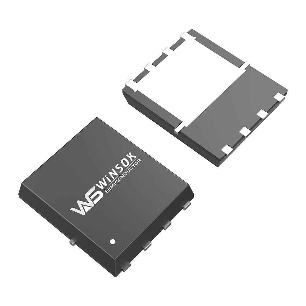
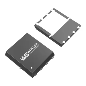
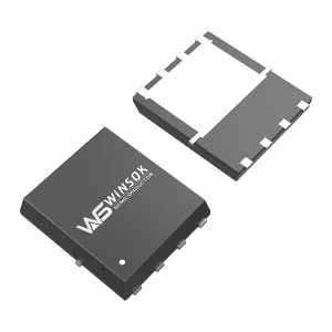
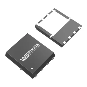
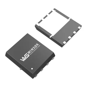
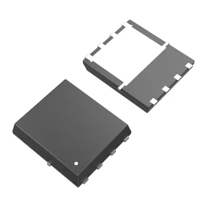
Custom WSD75N12GDN56 N-channel 120V 75A DFN5X6-8 WINSOK MOSFET Supplier, Product

Part Number:WSD75N12GDN56 BVDSS:120V ID:75A RDSON:6mΩ Channel:N-channel Package:DFN5X6-8

Product Description

Voltage 120V
🔌 Current 75A
🎛️ Resistance 6mΩ
⛓️ Channel N-Channel
📦 Package DFN5X6-8
Target Applications
  • Medical Equipment MOSFET
  • Drones MOSFET
  • PD Power Supplies MOSFET
  • LED Power Supplies MOSFET
  • Industrial Equipment MOSFET
Alternative Part Numbers
  • AOS MOSFET AON6226, AON6294, AON6298
  • AOS MOSFET AONS6292, AONS6692, AONS66923
  • PANJIT MOSFET PSMQC76N12LS1
Absolute Maximum Ratings
Symbol Parameter Rating Units
VDSS Drain-to-Source Voltage 120 V
VGS Gate-to-Source Voltage ±20 V
ID Continuous Drain Current (Tc=25℃) 75 A
ID Continuous Drain Current (Tc=70℃) 70 A
IDM Pulsed Drain Current 320 A
IAR Single pulse avalanche current 40 A
EASa Single pulse avalanche energy 240 mJ
PD Power Dissipation 125 W
TJ, Tstg Operating Junction and Storage Temperature Range -55 to 150
TL Maximum Temperature for Soldering 260
RθJC Thermal Resistance, Junction-to-Case 1.0 ℃/W
RθJA Thermal Resistance, Junction-to-Ambient 50 ℃/W
Electrical Characteristics (TA = 25℃ unless otherwise noted)
Symbol Parameter Test Conditions Min. Typ. Max. Units
VDSS Drain to Source Breakdown Voltage VGS=0V, ID=250µA 120 -- -- V
IDSS Drain to Source Leakage Current VDS = 120V, VGS= 0V -- -- 1 µA
IGSS(F) Gate to Source Forward Leakage VGS =+20V -- -- 100 nA
IGSS(R) Gate to Source Reverse Leakage VGS =-20V -- -- -100 nA
VGS(TH) Gate Threshold Voltage VDS=VGS, ID = 250µA 2.5 3.0 3.5 V
RDS(ON)1 Drain-to-Source On-Resistance VGS=10V, ID=20A -- 6.0 6.8 mΩ
gFS Forward Transconductance VDS=5V, ID=50A -- 130 -- S
Ciss Input Capacitance VGS = 0V VDS = 50V f = 1.0MHz -- 4282 -- pF
Coss Output Capacitance -- 429 -- pF
Crss Reverse Transfer Capacitance -- 17 -- pF
Rg Gate resistance -- 2.5 --
td(ON) Turn-on Delay Time ID =20A VDS = 50V VGS = 10V RG = 5Ω -- 20 -- ns
tr Rise Time -- 11 -- ns
td(OFF) Turn-Off Delay Time -- 55 -- ns
tf Fall Time -- 28 -- ns
Qg Total Gate Charge VGS =0~10V VDS = 50V ID =20A -- 61.4 -- nC
Qgs Gate Source Charge -- 17.4 -- nC
Qgd Gate Drain Charge -- 14.1 -- nC
IS Diode Forward Current TC =25 °C -- -- 100 A
ISM Diode Pulse Current -- -- 320 A
VSD Diode Forward Voltage IS=6.0A, VGS=0V -- -- 1.2 V
trr Reverse Recovery time IS=20A, VDD=50V dIF/dt=100A/μs -- 100 -- ns
Qrr Reverse Recovery Charge -- 250 -- nC
Frequently Asked Questions
❓ What are the primary specifications of the WSD75N12GDN56 MOSFET?
The WSD75N12GDN56 is an N-channel MOSFET designed for high performance with a Drain-to-Source voltage of 120V, continuous current capability of 75A, and a low typical on-resistance (RDS(ON)) of 6mΩ. It is housed in a compact DFN5x6-8 package.
❓ What applications can utilize the WSD75N12GDN56 MOSFET?
This N-channel MOSFET is highly optimized for power switching circuits and is commonly used in medical equipment, drones, PD power supplies, LED power drivers, and various types of industrial equipment.
❓ Are there equivalent replacement options for the WSD75N12GDN56?
Yes, compatible replacement equivalents include AOS MOSFET models such as AON6226, AON6294, AON6298, AONS6292, AONS6692, AONS66923, as well as the PANJIT MOSFET model PSMQC76N12LS1.
❓ What is the thermal resistance performance of this MOSFET?
The WSD75N12GDN56 shows efficient thermal characteristics with a Junction-to-Case thermal resistance (RθJC) of 1.0 ℃/W and a Junction-to-Ambient thermal resistance (RθJA) of 50 ℃/W.
❓ What are the operation and storage temperature limits?
The device is rated to operate safely within a broad junction and storage temperature range (TJ, Tstg) of -55 ℃ up to 150 ℃. The maximum temperature limit for soldering is 260 ℃.
❓ What are the input and output capacitance parameters for WSD75N12GDN56?
Under test conditions of VGS = 0V, VDS = 50V, and f = 1.0MHz, the typical Input Capacitance (Ciss) is 4282 pF, Output Capacitance (Coss) is 429 pF, and Reverse Transfer Capacitance (Crss) is 17 pF.

Related Products