Q
What are the key electrical characteristics of the WSK250N03 MOSFET?
The WSK250N03 is an N-channel MOSFET featuring a maximum drain-to-source voltage (VDS) of 30V, a continuous drain current (ID) of 250A, and an ultra-low on-resistance (RDS(ON)) of 1.8mΩ typical (2.5mΩ max) at 10V.
Q
What type of package does the WSK250N03 use?
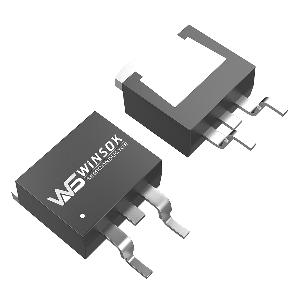
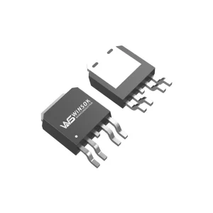
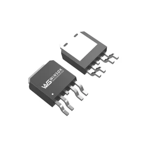
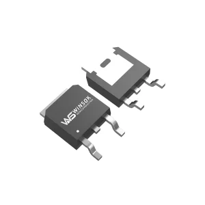
This MOSFET is housed in a TO-263-2L package, which is designed for high-power applications requiring excellent thermal dissipation and surface-mount compatibility.
Q
What are the suitable applications for this MOSFET?
It is ideal for a wide range of devices including e-cigarettes, wireless chargers, motor controllers, emergency power supplies, drones, medical equipment, car chargers, 3D printers, and general consumer electronics.
Q
What is the input capacitance (Ciss) of the WSK250N03?
The typical input capacitance (Ciss) of the WSK250N03 is 10,600 pF, which is essential for determining the gate drive requirements in switching circuits.
Q
Are there any compatible equivalent models for cross-referencing?
Yes, compatible cross-reference models include the AOS AOB1404L, AOB2140L, AOB2144L, and the POTENS PDH3960.
Q
How does the RDS(ON) vary with different gate-to-source voltages (VGS)?
At VGS = 10V, the RDS(ON) is 1.8mΩ (typical). At a lower gate drive of VGS = 4.5V, the RDS(ON) increases to 2.5mΩ (typical) and 3.5mΩ (maximum).
 Olukey