Olukey


1 / 4
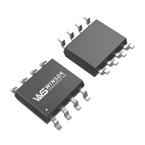
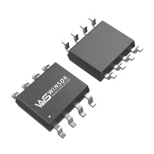
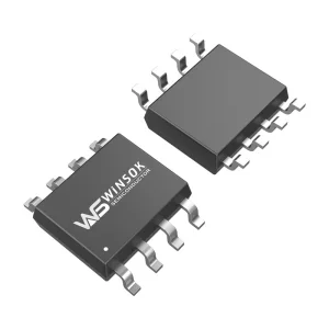
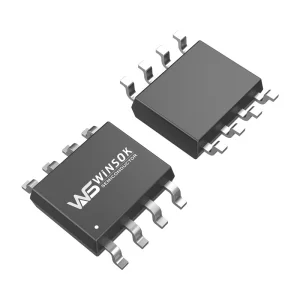
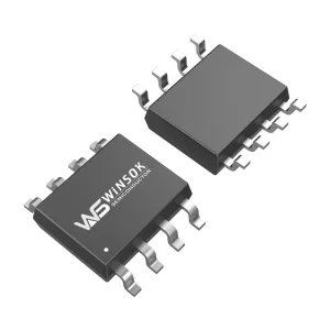
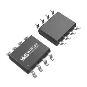
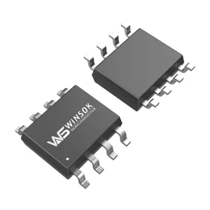
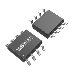
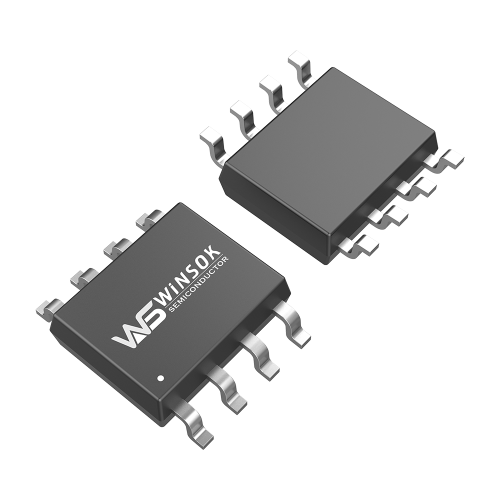
The WSP4953 is the highest performance Dual P-CH MOSFET with extreme high cell density, which provides excellent RDSON and gate charge for most of the synchronous buck converter applications. The WSP4953 meets the RoHS and Green Product requirements with full function reliability approved.
Designed to function across a wide range of international standard operating temperatures.
Original, brand new chips ensure reliable performance in your electronic designs.
International standard dissipation power ensures highly efficient chip operation.
Offered as customized options, allowing these chips to be tailored to specific project needs.
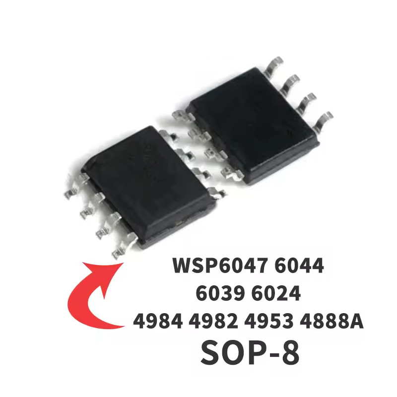
Arduino Chip | Sm26043. Includes 5 distinct SOP8 chips, catering to diverse electronic projects.
| Symbol | Parameter | Rating | Units |
|---|---|---|---|
| VDS | Drain-Source Voltage | -30 | V |
| VGS | Gate-Source Voltage | ±20 | V |
| ID@TC=25ºC | Continuous Drain Current, -VGS @ -10V¹ | -5.3 | A |
| ID@TC=100ºC | Continuous Drain Current, -VGS @ -10V¹ | -4.6 | A |
| IDM | Pulsed Drain Current² | -12 | A |
| PD@TC=25ºC | Total Power Dissipation³ | 1.5 | W |
| TSTG | Storage Temperature Range | -55 to 150 | ºC |
| TJ | Operating Junction Temperature Range | -55 to 150 | ºC |
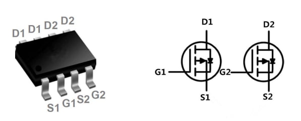
The WSP4953 is optimized for high-frequency point-of-load synchronous buck converters in motherboards (MB), notebooks (NB), UMPCs, VGA cards, networking DC-DC power systems, and load switches.
The WSP4953 can operate across a junction and storage temperature range from -55ºC up to 150ºC, making it stable under diverse environment conditions.
Yes. The WSP4953 is fully approved under RoHS regulations and qualifies as a Green Product with certified full-function reliability.
The product lineup includes 5 distinct SOP8 package configurations designed to support versatile electronic system integrations and projects like Arduino.
The maximum Drain-Source Voltage (VDS) is rated at -30V, and the Gate-Source Voltage (VGS) limit is ±20V.
Its extreme high cell density configuration delivers exceptionally low RDSON and optimized gate charge parameters, which significantly minimizes power loss in buck converter circuits.