Olukey
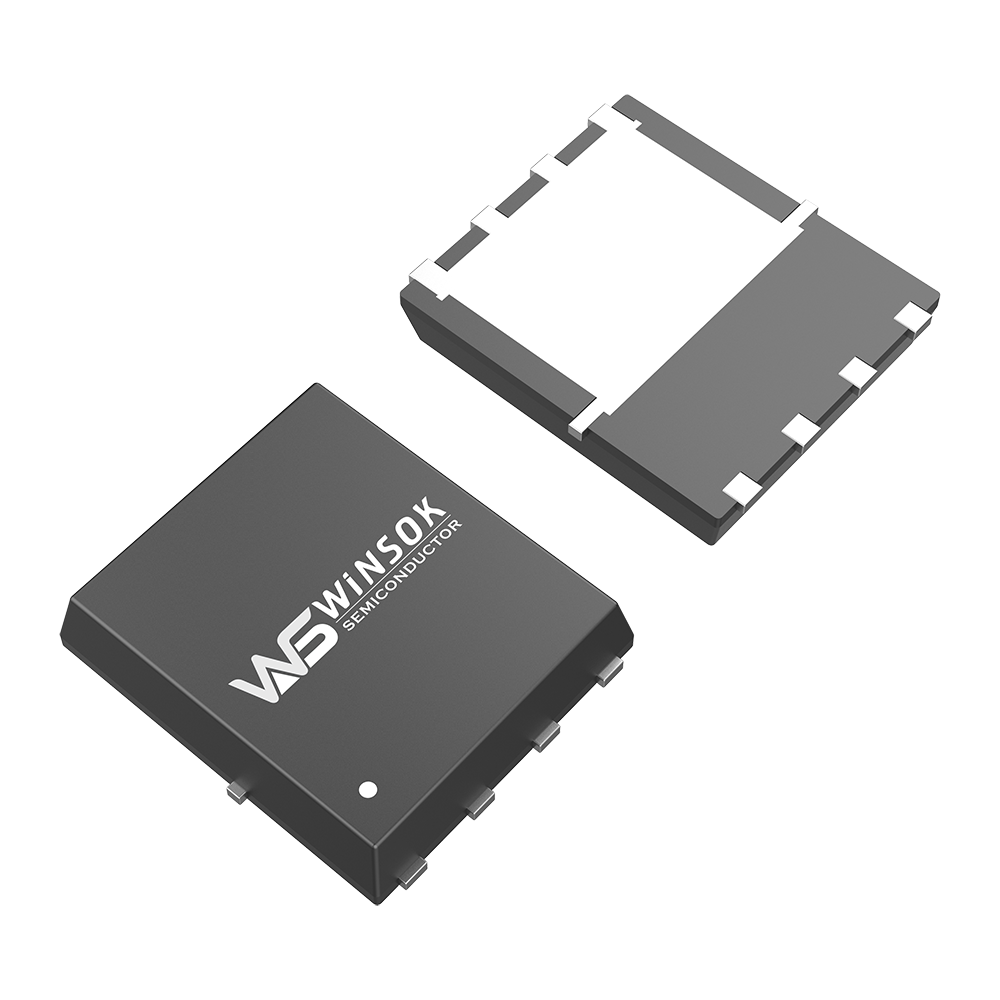
1 / 1
Part Number
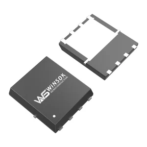
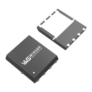
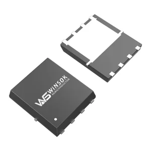
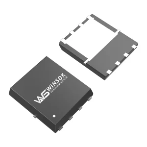
WSD6040DN56
Drain-Source Voltage (Vds)
60V
Continuous Current (Id)
36A
On-Resistance (Rds(on))
14mΩ
Channel Type
N-Channel
Package Type
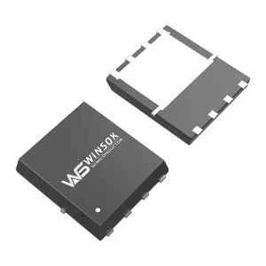
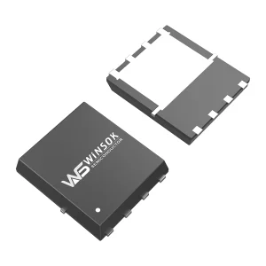
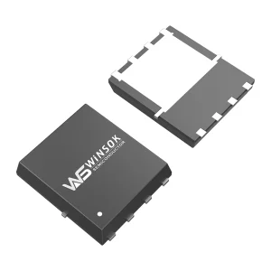
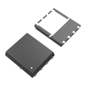
DFN5X6-8
| Symbol | Parameter | Rating | Units | ||
|---|---|---|---|---|---|
| VDS | Drain-Source Voltage | 60 | V | ||
| VGS | Gate-Source Voltage | ±20 | V | ||
| ID | Continuous Drain Current | TC=25°C | 36 | A | |
| TC=100°C | 22 | ||||
| ID | Continuous Drain Current | TA=25°C | 8.4 | A | |
| TA=100°C | 6.8 | ||||
| IDM a | Pulsed Drain Current | TC=25°C | 140 | A | |
| PD | Maximum Power Dissipation | TC=25°C | 37.8 | W | |
| TC=100°C | 15.1 | ||||
| PD | Maximum Power Dissipation | TA=25°C | 2.08 | W | |
| TA=70°C | 1.33 | ||||
| IAS c | Avalanche Current, Single pulse | L=0.5mH | 16 | A | |
| EAS c | Single Pulse Avalanche Energy | L=0.5mH | 64 | mJ | |
| IS | Diode Continuous Forward Current | TC=25°C | 18 | A | |
| TJ | Maximum Junction Temperature | 150 | ℃ | ||
| TSTG | Storage Temperature Range | -55 to 150 | ℃ | ||
| RθJA b | Thermal Resistance Junction to ambient | Steady State | 60 | ℃/W | |
| RθJC | Thermal Resistance-Junction to Case | Steady State | 3.3 | ℃/W | |
| Symbol | Parameter | Conditions | Min. | Typ. | Max. | Unit | |
|---|---|---|---|---|---|---|---|
| Static | |||||||
| V(BR)DSS | Drain-Source Breakdown Voltage | VGS = 0V, ID = 250μA | 60 | V | |||
| IDSS | Zero Gate Voltage Drain Current | VDS = 48 V, VGS = 0V | 1 | µA | |||
| TJ=85°C | 30 | ||||||
| IGSS | Gate Leakage Current | VGS = ±20V, VDS = 0V | ±100 | nA | |||
| On Characteristics | |||||||
| VGS(TH) | Gate Threshold Voltage | VGS = VDS, IDS = 250µA | 1 | 1.6 | 2.5 | V | |
| RDS(on) d | Drain-Source On-state Resistance | VGS = 10V, ID = 25A | 14 | 17.5 | mΩ | ||
| VGS = 4.5V, ID = 20A | 19 | 22 | mΩ | ||||
| Switching | |||||||
| Qg | Total Gate Charge | VDS=30V VGS=10V ID=25A |
42 | nC | |||
| Qgs | Gate-Source Charge | 6.4 | nC | ||||
| Qgd | Gate-Drain Charge | 9.6 | nC | ||||
| td (on) | Turn-on Delay Time | VGEN=10V VDD=30V ID=1A RG=6Ω RL=30Ω |
17 | ns | |||
| tr | Turn-on Rise Time | 9 | ns | ||||
| td(off) | Turn-off Delay Time | 58 | ns | ||||
| tf | Turn-off Fall Time | 14 | ns | ||||
| Rg | Gate resistance | VGS=0V, VDS=0V, f=1MHz | 1.5 | Ω | |||
| Dynamic | |||||||
| Ciss | Input Capacitance | VGS=0V VDS=30V, f=1MHz |
2100 | pF | |||
| Coss | Output Capacitance | 140 | pF | ||||
| Crss | Reverse Transfer Capacitance | 100 | pF | ||||
| Drain-Source Diode Characteristics and Maximum Ratings | |||||||
| IS | Continuous Source Current | VG=VD=0V , Force Current | 18 | A | |||
| ISM | Pulsed Source Current | 35 | A | ||||
| VSD d | Diode Forward Voltage | ISD = 20A , VGS=0V | 0.8 | 1.3 | V | ||
| trr | Reverse Recovery Time | ISD=25A, dISD/dt=100A/µs | 27 | ns | |||
| Qrr | Reverse Recovery Charge | 33 | nC | ||||
What are the primary specifications of the WSD6040DN56 MOSFET?
The WSD6040DN56 is an N-channel MOSFET designed with a drain-source voltage (VDS) of 60V, a continuous current rating (ID) of 36A, and a typical drain-source on-state resistance (RDS(on)) of 14mΩ at VGS=10V. It is housed in a DFN5X6-8 package.
What applications are suitable for the WSD6040DN56 MOSFET?
It is highly optimized for various applications including wireless charging, e-cigarettes, motor drivers, drones, medical care equipment, car chargers, controllers, digital products, small household appliances, and other consumer electronics.
Which MOSFETs can be used as equivalents or cross references for the WSD6040DN56?
Compatible cross-reference models include AOS MOSFETs (AON6264C, AON6264E, AON6266E, AONS6662), STMicroelectronics (STL8DN6LF6AG), PANJIT (PSMQC12N6LS1), and POTENS Semiconductor (PDC6964X).
What is the gate threshold voltage (VGS(TH)) range for WSD6040DN56?
The gate threshold voltage (VGS(TH)) has a minimum rating of 1.0V, a typical value of 1.6V, and a maximum rating of 2.5V when measured under conditions of VGS = VDS and IDS = 250µA.
What are the thermal parameters for the WSD6040DN56 MOSFET?
The thermal resistance from junction to ambient (RθJA) is 60 ℃/W under steady-state conditions, while the thermal resistance from junction to case (RθJC) is 3.3 ℃/W under steady-state conditions.
What is the maximum operating junction temperature for this device?
The WSD6040DN56 MOSFET supports a maximum operating junction temperature (TJ) of 150°C and a storage temperature range (TSTG) from -55°C to 150°C.