Premium low-to-high voltage MOSFET solutions optimized for high-frequency flyback converters and synchronous rectification.

In the contemporary consumer electronics ecosystem, the push for smaller, more efficient, and faster-charging systems has created a massive paradigm shift. High-power-density USB-C Power Delivery (PD 3.0 / PD 3.1) adapters ranging from 20W to 240W require advanced power switches that minimize thermal dissipation while maintaining exceptional efficiency at elevated frequencies. This is where custom MOSFETs designed specifically for fast chargers play an indispensable role.
While newer wide-bandgap (WBG) technologies like Gallium Nitride (GaN) have dominated headlines for premium adapters, Silicon (Si) MOSFETs remain the absolute backbone of the global charging market. Innovations in superjunction architecture and low gate charge (Qg) packaging allow modern silicon MOSFETs to meet strict energy star ratings and operating parameters at a fraction of the cost of GaN, providing the optimal balance of commercial viability and high performance.
Fast chargers typically employ one of two main structural topologies where MOSFETs dictate overall efficiency:

HONGKONG Olukey INDUSTRY CO., LIMITED is an industry-leading integrated solution provider focusing on the holistic provisioning of electronic components. Our dynamic product ecosystem is engineered around three core high-tech vectors: WINSOK MOSFETs, Cmsemicon MCUs, and bespoke PCBA circuit board solution development.
Currently, Olukey Industry's advanced portfolios are extensively integrated across various mission-critical sectors including automotive electronics, military electronics, smart industrial automation, new energy infrastructure, smart medical devices, 5G networking equipment, the Internet of Things (IoT), smart home ecosystems, and high-performance consumer electronics.
By leveraging strategic partnerships and holding global general agent status with major original factories, we maintain a dominant presence within the Asia-Pacific market. Our core mandate is to assist global OEMs and ODMs in bringing highly reliable, energy-efficient products to market through simplified sourcing, superior technical field application engineering (FAE) support, and robust quality guarantees.
A breakdown of our manufacturing capabilities, engineering advantages, and cross-reference versatility.
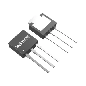
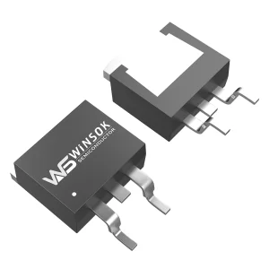
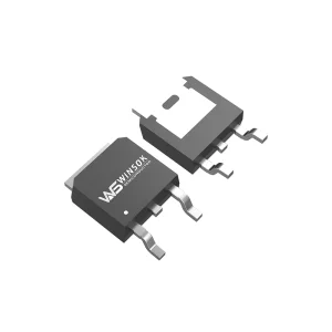
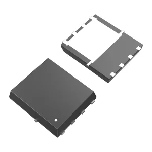
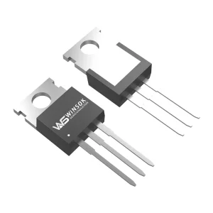
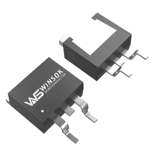
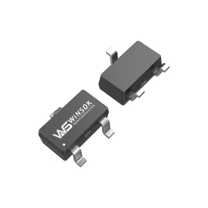
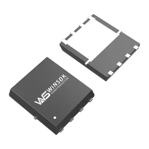
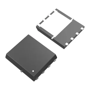
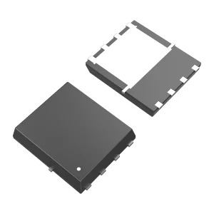
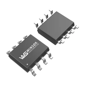
Over 40 package styles including ultra-compact DFN3X3-8, thermal-efficient DFN5X6-8, high-power TO-252, TO-263, SOP-8, SOT-23, and TO-220, matching all standard industrial footprints.
Comprehensive low-to-high voltage range offerings: 15V, 20V, 30V, 40V, 60V, 80V, 100V, 120V, 150V, 200V, 250V, 300V, 400V, 500V, 600V, and 650V options for standard power topologies.
Direct parametric replacements for premium global brands. For example, our DFN5X6-8 N-channel series directly replaces industry-standard parts such as FDMC81DCCM, PSMN1R7-3YL, and TPH1R43NL.
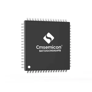
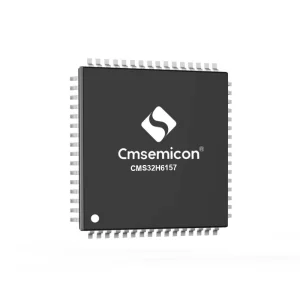
Access to Cmsemicon microcontrollers (LQFP64, LQFP80, LQFP100 packages) allows for complete system-level integration of charging protocols, safety limits, and gate driving logic.

In the semiconductor supply chain, geographical positioning and logistical infrastructure determine commercial competitiveness. Relying on OLUKEY Industry's central operations based in Hong Kong and Shenzhen—the global epicenter of consumer electronics and semiconductor assembly—clients secure direct lines of supply that bypass typical supply bottlenecks.
By leveraging localized fabrication facilities and packaging centers, we ensure short lead times, rapid prototype iterations, and highly competitive pricing. This ecosystem enables us to respond dynamically to sudden market demand spikes, such as the rapid transition to high-wattage GaN-Silicon hybrid fast chargers. With more than 600 models in active production, we maintain high safety stock levels for common power-stage MOSFETs, allowing global partners to scale up operations without the risk of line-down scenarios.
We believe that trust is earned through transparency and rigorous testing. Every batch of Winsok MOSFETs undergoes comprehensive testing protocols, including:

Navigating different local safety standards (such as UL, CE, CCC, PSE, and KC mark requirements) demands deep component-level compliance. When implementing a MOSFET into a fast charger's power path, the primary safety and EMI concerns revolve around leakage current, thermal margins, and high-frequency switching noise.
We provide localized engineering support to help optimize layout designs for EMI reduction. High $dV/dt$ and $dI/dt$ transitions inside fast chargers can cause significant electromagnetic interference. By matching the optimal internal gate resistance ($Rg$) and selecting the correct packaging (such as replacing wire-bonded SOP-8 with clip-bonded DFN5x6 to lower parasitic inductance), our field application engineers (FAEs) help developers clear EMC tests on their first attempt.
All Winsok MOSFET solutions comply strictly with environmental and supply regulations, including RoHS 2.0, REACH, and Halogen-Free requirements. This clean material profile ensures that chargers built using our MOSFETs can be seamlessly imported and distributed in strict markets, including the European Union and North America.

Modern power systems are highly complex, requiring synchronous coordination between the digital control unit (MCU) and the analog power switches (MOSFETs). Our integrated component supply chain addresses these challenges comprehensively.
From 20W smartphone mini-chargers to 140W laptop chargers. The combination of Cmsemicon MCUs (running custom PD negotiation firmware) and low-Qg Winsok MOSFETs provides smooth voltage transitions and minimal thermal signatures.
On-board chargers and high-power USB ports integrated into car consoles. These systems require ruggedized MOSFETs with high avalanche resistance to withstand the harsh electrical transients common in automotive power lines.
Compact, embedded power supplies for smart wall switches, wireless routers, and IoT hubs. The focus here is on standby power reduction, requiring MOSFETs with extremely low off-state leakage currents.

Addressing core design challenges, cross-referencing capabilities, and structural optimizations.
A reference guide comparing package types and voltage characteristics for fast charger implementation.
Choosing the correct packaging is just as critical as selecting the silicon parameters. To ensure long operating lifetimes, power engineers must carefully evaluate the thermal dissipation path. For high-density fast chargers, the choice between DFN, TO-252, and SOP packaging determines the mechanical envelope and overall cooling requirements of the adapter shell.
For example, low-voltage high-current designs use the DFN5x6 package to minimize conduction losses at high current densities. On the other hand, primary switches in offline adapters often utilize TO-220 or TO-251S packages due to their superior thermal performance under high-voltage stresses.

High-reliability dual-channel, high-voltage, and specialized packaging solutions for diverse system requirements.
 Olukey