Olukey







Technical Whitepaper: MOSFET Design Challenges in USB-C PD Chargers
Evaluating evolution, semiconductor structures, loss mechanisms, and integration solutions in advanced charger architectures.
1. The Evolution of USB-C PD Chargers & Market Dynamics
The consumer electronics market has experienced a significant shift with the introduction of USB Power Delivery (USB-C PD) and Programmable Power Supply (PPS) protocols. Charging infrastructures have scaled from standard 5W/10W linear topologies to high-power density designs reaching 65W, 100W, and even up to 240W via the Extended Power Range (EPR) specifications (delivering up to 48V at 5A). This growth requires high switching frequencies to reduce the overall size of passive components like transformers and output capacitors.
Consequently, the performance demands placed on power MOSFETs have increased. In modern fast-charging architectures, MOSFETs are no longer simple switching elements; they are highly optimized silicon or wide-bandgap (WBG) devices that manage primary high-voltage switching, secondary synchronous rectification (SR), and VBUS load switching. Minimizing parasitic parameters like gate charge ($Q_g$), gate-drain charge ($Q_{gd}$), and drain-source on-resistance ($R_{DS(on)}$) is critical to maintaining thermal efficiency above 93% in compact enclosures.
2. Technical Obstacles in Modern Charger Architecture
To construct a highly efficient, space-constrained charging brick, design engineers face multiple electrical and thermal hurdles:
- Primary Switch Losses: Operating at frequencies between 100kHz and 500kHz to decrease magnetics size increases frequency-related switching losses ($P_{sw}$). The primary high-voltage switch must feature minimal output capacitance ($C_{oss}$) to reduce energy storage ($E_{oss}$) and enable Zero Voltage Switching (ZVS) in Quasi-Resonant (QR) or Active Clamp Flyback (ACF) topologies.
- Secondary Synchronous Rectification (SR) Challenges: Replacing traditional Schottky diodes with SR MOSFETs significantly improves efficiency. However, the SR MOSFET faces high di/dt stress and gate-drive timing challenges. A delayed turn-off can trigger cross-conduction, while premature turn-off directs current through the body diode, increasing thermal load.
- EMI and dv/dt Immunity: High switching speeds ($dv/dt$) induce capacitive currents into the control circuit, resulting in electromagnetic interference (EMI) and gate-bounce issues. Robust gate-drive circuitry combined with internal gate-resistance parameters is required to prevent unintended turn-on events.

3. Global Procurement Trends & Supply Chain Resilience
Industrial purchasing departments face volatile supply conditions when sourcing high-quality power devices. Standard commodity chips struggle with consistent performance and availability, forcing Tier-1 OEMs to focus on:
- Second-Source Qualification: High-volume manufacturers must qualify high-quality alternative sources to guard against primary supplier line stoppages. Olukey Industry resolves this bottleneck by stocking fully compatible, low $R_{DS(on)}$ WINSOK MOSFETs that meet or exceed standard industry specs.
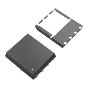
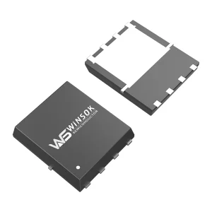
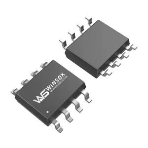
- Optimized Lead Times: Maintaining continuous stock buffers of fast-switching MOSFETs in standard packages like DFN3X3-8, DFN5X6-8, and SOP-8 helps manufacturers avoid shipping delays and scale production to meet market demands.
- Full Application Support: Having local Field Application Engineers (FAEs) to troubleshoot gate oscillation, thermal hotspots, and EMI compliance speeds up development timelines and reduces time-to-market.
4. Olukey & WINSOK Co-Designed Solutions
By combining WINSOK's silicon production with Cmsemicon's MCU capabilities and Hongkong Olukey Industry's PCBA design, we offer full-system solutions for fast-charging adapters. Rather than sourcing components separately, clients receive a pre-designed, tested subsystem:
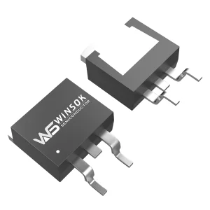
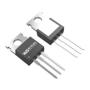
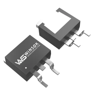
- Primary Switched Topologies: Our high-voltage MOSFETs (up to 650V in TO-263 and TO-220 packages) provide reliable margins against primary-side voltage spikes.
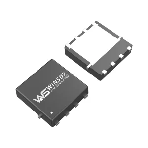
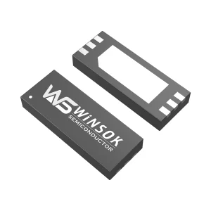
- Synchronous Rectification (SR): Low-voltage, high-current N-channel MOSFETs (30V to 100V in DFN3x3 and DFN5x6 packages) enable low conduction losses in secondary rectification systems.
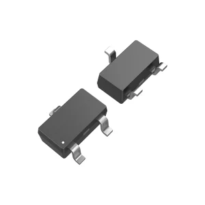
- USB-C VBUS Switch: Low $R_{DS(on)}$ P-channel and N-channel devices (20V to 40V) protect downstream mobile devices against high surges.
This integration ensures compatible gate-drive voltage matching between the microcontroller and the MOSFET, mitigating gate-drive losses and stabilizing the overall circuit.

5. Future Roadmap & Technology Innovations
The power electronics industry is moving toward higher-frequency architectures. While wide-bandgap (GaN and SiC) devices serve ultra-premium chargers, advanced silicon MOSFETs remain the standard for high-volume, cost-sensitive 20W to 140W products due to their reliability, cost structure, and mature manufacturing processes.
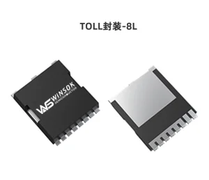
Our upcoming product generation focuses on reducing parasitic capacitances through advanced trench technology and package modifications. By transitioning to clip-bonded DFN and TOLL packages, we reduce package-level parasitic inductances, enabling clean switching waveforms at frequencies above 300kHz.