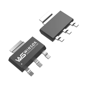
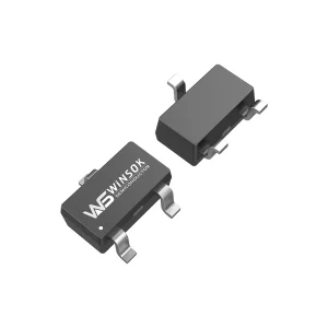
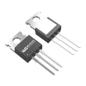
High reliability and extreme thermal performance engineered for advanced protection circuits. Select models below to request samples or place OEM/ODM orders.
In modern lithium-ion and lithium-iron-phosphate (LiFePO4) battery management systems (BMS), power MOSFETs function as safety switches. They must operate flawlessly under extreme conditions to prevent hazardous events such as thermal runaway, overcharging, over-discharging, and short circuits. Choosing the right power MOSFET is critical to achieving high efficiency, minimal heat dissipation, and long-term reliability.
The efficiency of a battery protection circuit is heavily dependent on the On-Resistance ($R_{DS(on)}$) of the MOSFETs used. When current flows through the protection switch during charge or discharge cycles, power is dissipated as heat, governed by the formula $P = I^2 \times R_{DS(on)}$. A higher resistance leads to thermal bottlenecks, reducing overall system efficiency and accelerating battery degradation.
Our ultra-low RDS(on) MOSFETs are engineered to minimize static power losses, enabling high-density battery packs to operate cooler and safer across wide load spectrums.
Additionally, parameters like Gate Charge ($Q_g$) and Safe Operating Area (SOA) must be meticulously evaluated. A lower Gate Charge enables faster switching, reducing transient switching losses. A robust SOA ensures the device can withstand transient over-current events before the driver circuit triggers a complete shutdown.


HONGKONG Olukey INDUSTRY CO., LIMITED is a premier global solution provider specializing in advanced electronic component architectures. We deliver comprehensive system solutions across three core product portfolios: WINSOK MOSFET, Cmsemicon MCU, and custom PCBA circuit board design.
By leveraging our deep-seated supply chain alliances and direct factory channels in the Asia-Pacific region, Olukey provides a continuous pipeline of high-performance components to global manufacturers. Our applications span automotive systems, industrial automation, telecommunications (5G/IoT), defense systems, medical devices, and high-reliability consumer electronics. We focus on engineering-driven distribution, assisting developers from initial prototyping to high-volume manufacturing.
WINSOK MOSFETs provide design engineers with an extensive selection of low-to-medium voltage power components. Our engineering support includes a comprehensive cross-reference database for effortless replacement of expensive legacy brands. By combining our robust component design with competitive pricing and rapid prototyping programs (including free evaluation samples), we help accelerate your project's development cycle.
Furthermore, our technical partnership with Cmsemicon allows us to deliver integrated microcontroller and power stage solutions. This streamlined architecture optimizes space and reduces the Bill of Materials (BOM) in smart battery systems, motor controllers, and automotive subsystems.
Reliable performance, robust supply lines, and dedicated engineering support make Olukey the preferred partner for modern power designs.



China’s semiconductor ecosystem has transitioned from basic assembly to advanced power electronics development. By leveraging cleanroom facilities, advanced photolithography, and highly automated testing backends in locations like Shenzhen and Hong Kong, local manufacturers ensure high-volume yields.
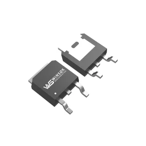
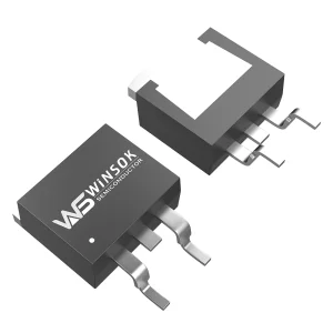
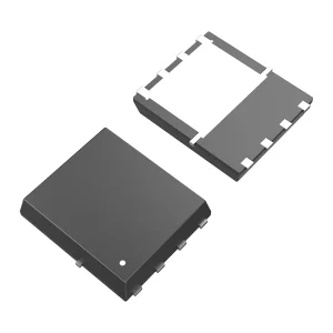
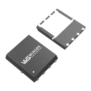
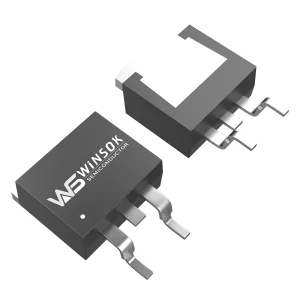
This integrated supply chain enables rapid turnaround times from silicon ingot slicing to final packaged parts (such as DFN5x6-8L and TO-252). Global procurement teams benefit from reduced freight times, direct communication, and flexible volume pricing, allowing agile companies to maintain lean inventories.
Traditional battery protection circuits used simple analog comparator ICs to toggle MOSFET gates. Today's systems employ smart microcontrollers (such as Cmsemicon MTP/RISC families) to execute state-of-health (SOH) and state-of-charge (SOC) algorithms.
This evolution requires MOSFETs to maintain low threshold drift and operate reliably at low gate drive voltages. As EV battery modules switch to higher series cells, the power switches must maintain balanced parameters to prevent differential heating inside the battery packs.
Application environments vary significantly across regions. For example, high-humidity, high-salt coastal areas require robust packaging sealing, while harsh industrial zones demand high ESD threshold parameters.
By designing MOSFETs with thick passivation layers and optimized gate structures, we reduce localized degradation from atmospheric ingress. This ensures long-term reliability in applications ranging from grid energy storage systems to rugged agricultural drones.


Practical engineering insights for selecting, designing, and optimizing battery management systems with advanced power switches.
To select the optimum $R_{DS(on)}$, determine the maximum continuous discharge current ($I_{max}$) and the maximum allowable junction temperature ($T_{j,max}$). Calculate power dissipation using $P = I^2 \times R_{DS(on)(at\ T_j)}$. Using the formula $T_j = T_a + P \times R_{\theta JA}$ (where $R_{\theta JA}$ is the junction-to-ambient thermal resistance), you can determine the maximum tolerable $R_{DS(on)}$ at operating temperatures. It is recommended to include a safety margin of at least 30% to account for transient load spikes and variations in ambient temperature.
N+P complementary channel MOSFETs combine both types of switch into a single package. This enables simplified control topologies without requiring isolated charge-pump gate drivers. In USB power chargers and low-voltage wearable battery configurations, the P-channel device can control the high-side power path, while the N-channel handles the low-side grounding or load switching. This configuration reduces overall component count, saves board space, and simplifies routing.
When paralleling power MOSFETs, parameters like threshold voltage ($V_{GS(th)}$) and parasitic trace layout must be closely matched to prevent current mismatch and thermal imbalances during switching transitions. If one device switches on faster than the others, it temporarily carries the entire load current, which can lead to localized failures. Using individual gate resistors helps prevent high-frequency oscillation, and routing the power traces symmetrically ensures equal parasitic inductances and balanced current sharing.
DFN5x6 package designs offer significantly lower package resistance and inductance than leaded TO-252 packages. By utilizing copper-clip die attach technology, DFN packages provide a direct, low-resistance thermal path to the PCB. This design minimizes space requirements while offering equivalent or superior thermal performance. This makes DFN packages ideal for modern, space-constrained battery protection modules.
Engineered to deliver high ruggedness and efficiency in demanding power electronics environments. Request your free evaluation sample kit today.
 Olukey