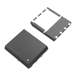
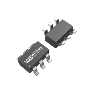
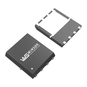
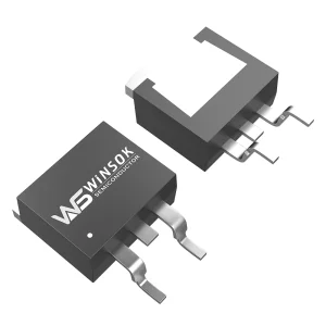
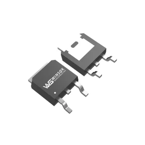
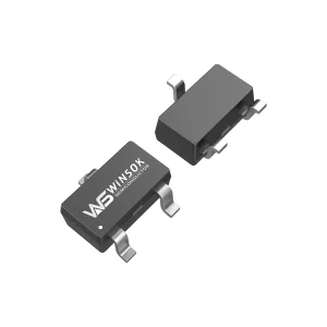
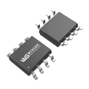
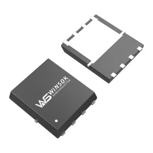
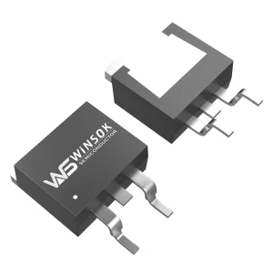
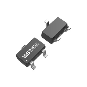
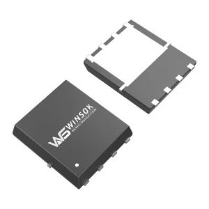
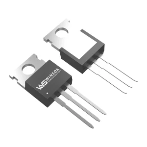
Explore our primary high-density packaging configurations offering ultra-low conduction losses and robust Safe Operating Areas (SOA).
Understanding the Critical Physics of Thermal Stability, Gate Charge, and R_DS(on) Matching in High-Capacity Battery Protection Circuits.
Modern lithium-ion battery packs, spanning from 1S/2S systems in smartphones to multi-cell arrays (10S to 20S) in light electric vehicles (LEVs) and energy storage systems (ESS), demand unparalleled reliability from their switching components. In these designs, power MOSFETs act as the primary safety gatekeeper, interrupting high-fault currents during overcurrent, short-circuit, or overtemperature events.
The primary design parameter is minimizing $R_{DS(on)}$ (Static Drain-Source On-State Resistance) to reduce continuous conduction loss ($P_{loss} = I_{RMS}^2 \times R_{DS(on)}$). In high-density layouts, even a fraction of a milliohm variation can translate to critical thermal gradients that degrade the lithium cells' lifespan. Modern Trench-gate and Split-gate technologies allow us to pack millions of conductive channels into micro-scale footprints (such as DFN5x6 and SOT-23-6L), driving $R_{DS(on)}$ down to sub-milliohm levels.
When the BMS triggers an emergency shutdown, the MOSFET must turn off extremely fast while absorbing the inductive energy stored in the battery leads and routing paths. This transient stress is governed by the MOSFET's Safe Operating Area (SOA) and its single-pulse avalanche rating ($E_{AS}$).
A typical failure mode during short-circuit interruption is thermal hotspotting. Under high VDS and ID conditions, local areas within the silicon die can enter a positive feedback thermal cycle, leading to catastrophic gate-oxide rupture. By deploying optimized cell-spacing designs and robust metal layers on top of the silicon die, our alternative MOSFETs guarantee excellent current distribution, mitigating the risks of localized hotspotting during abrupt current drop-offs.
| Industry Standard Brand Part Number | WINSOK Direct Drop-in Equivalent | Package Type | V_DS (V) | R_DS(on) Typ. @10V (mΩ) | Application Target | Cross-Reference Status |
|---|---|---|---|---|---|---|
| AON6226 / AONS6292 | WSD3075DN56 | DFN5X6-8L | 30V | < 2.1 mΩ | 1S-3S Power Bank, Laptop BMS | Pin-to-Pin Perfect Match |
| AOSP66406 / FDS8842NZ | WSD6040DN56 | DFN5X6-8 | 60V | < 7.5 mΩ | E-Bike Charger Protection, E-Scooter BMS | Pin-to-Pin Perfect Match |
| Si4840BDY | WST8205 | SOT-23-6L | 20V | < 19 mΩ | Single-Cell Lithium Protectors (PCM) | Direct Equivalent |
| AONS6692 / AONS66923 | WSK280N06G6 | TO-263-2L | 60V | < 1.3 mΩ | High-Power Cordless Tools, AGVs, Drones | Compatible Alternative |
Why Tier-1 OEMs and Electronics Manufacturers are Actively Transitioning to Certified Second-Source & Drop-in MOSFET Equivalents.
Geopolitical tensions, component allocations, and silicon shortages have highlighted the vulnerability of single-sourcing strategies. By integrating approved cross-reference equivalents early in the design stage, procurement teams can instantly switch suppliers when lead times fluctuate, preventing factory downtime.
High-volume consumer electronics, such as smart vacuum cleaners, power banks, and personal mobility devices, operate on razor-thin margins. WINSOK MOSFET equivalents provide a 30% to 50% cost advantage over legacy tier-1 brands without sacrificing reliability or thermal performance, significantly lowering BOM costs.
Our engineering-first model supports rapid validation. We offer comprehensive engineering sample kits free of charge, along with detailed qualification packets including thermal imaging, ESD test ratings, and continuous current sweep curves to accelerate your testing process.
How our components drive performance from low-voltage micro-wearables to high-power smart energy grids.
BMS Topology: 1S-2S Configuration
Optimal Packages: WST8205 SOT-23-6L, DFN3X3-8
Focuses on ultra-low gate threshold voltage ($V_{GS(th)}$) to allow full turn-on under weak battery conditions, ensuring precise protection even at critical depletion stages.
BMS Topology: 10S-20S High Power Packs
Optimal Packages: DFN5X6-8L, TO-252, TO-263
Designed for heavy inductive loads. Delivers robust avalanche energy ($E_{AS}$) performance and low thermal resistance ($R_{\theta JC}$) to prevent failures from back-EMF spikes during heavy deceleration or motor stalls.
BMS Topology: High-Voltage Multi-string Systems
Optimal Packages: TO-220, TO-263-2L, Custom High Voltage
Engineered for extended operating lifespans. Minimizes gate leakage current and offers robust static ratings, maintaining safety controls over decades of continuous service.
HONGKONG Olukey INDUSTRY CO., LIMITED is a leading solution provider focusing on the overall solution of electronic product components. Our core business lines encompass three highly integrated segments: WINSOK MOSFET, Cmsemicon MCU, and comprehensive PCBA circuit board solution development.
At present, Olukey Industry's advanced solutions are widely implemented in automotive electronics, military electronics, smart industrial automation, new energy systems, smart medical equipment, 5G communications infrastructure, the Internet of Things (IoT), smart home ecosystems, and high-tier consumer electronics.
Relying on the robust advantages of being global general agents of major original factories, we base our key operations in the fast-growing Asia-Pacific market. By providing customers with state-of-the-art electronic components backed by comprehensive premium services, we assist manufacturers in production quality enhancement and provide holistic support from concept to mass production.

Over the years, our organization has established a solid market presence based on reputation, adhering to the core principle of "quality first, service first." We maintain strong collaborative relationships with top-tier high-tech companies and key semiconductor foundries worldwide.
Our core product advantages for WINSOK MOSFETs focus on medium and low voltage ranges: 15V, 20V, 30V, 40V, 60V, 80V, 100V, 120V, 150V, 200V, 250V, 300V, 400V, 500V, 600V, and 650V. These are housed in diverse, high-reliability packages including DFN3X3-8, DFN5X6-8, TO-252, TO-263, SOP-8, SOT-23, TO-220, and more. With over 600 models and 40 packages, we cover the majority of medium-to-low voltage MOSFET market requirements.
Coupled with microcontrollers from Cmsemicon MCU, a company founded in Shenzhen with deep R&D experience, we provide a complete system-level solution. Becoming a global high-value agent is our ultimate target, driven by our corporate values: "Pragmatism, Win-win, Service, and Responsibility." We work hand-in-hand with our global manufacturing partners to explore larger markets and drive semiconductor innovation.






Underpinning our E-E-A-T credentials with advanced laboratory testing, certification standards, and engineering validation.
Our partner manufacturing facilities operate under certified ISO9001 quality management systems. Selected product lines designed for the automotive sector also conform to AEC-Q101 testing parameters to guarantee stable operations in high-vibration and extreme temperature environments.
All semiconductor components, package substrates, lead frames, and molding compounds conform to the latest RoHS Directive and REACH SVHC regulations, ensuring environmental compliance for exports to Europe and the Americas.
Our dedicated engineering labs perform scanning electron microscopy (SEM), X-ray package inspection, and scanning acoustic tomography (SAT) on every batch, maintaining strict control over bonding wires and silicon die attach processes.
Answers to complex engineering and procurement queries regarding product replacement, testing parameters, and compliance.
When selecting a drop-in equivalent, match these primary electrical parameters: Drain-Source Voltage ($V_{DS}$) must be equal to or greater than the original; Gate-Source Voltage ($V_{GS}$) absolute max ratings must match; Static Drain-Source On-Resistance ($R_{DS(on)}$) should be equal to or lower than the original to prevent excess thermal dissipation. Finally, verify the package footprint (e.g., DFN5x6-8L to DFN5x6-8L) and pinout to ensure it fits onto the existing PCB without layout adjustments.
We supply engineering departments with free validation samples for qualified BMS projects. You can contact our sales team with your target part numbers, estimated monthly/annual production volumes, and project specifications. Sample shipments typically go out within 2 to 5 business days, complete with data sheets and testing guidelines.
Yes. Our N-channel and P-channel MOSFETs feature high avalanche ruggedness ($E_{AS}$) and robust Safe Operating Areas (SOA). These characteristics enable the device to handle current surges during BMS short-circuit validation tests before the protective MCU triggers the gate shutdown loop.
Package selection affects the thermal dissipation capability ($R_{\theta JC}$) and current-handling limits of the bond wires. DFN5x6 packages are popular in compact designs due to their low profile and bottom-side thermal pads, while TO-252 and TO-263 packages are preferred in high-power applications (such as power tools and LEVs) where physical heatsinks or heavy copper planes are used to dissipate heat.
Select from our wide-ranging inventory configurations to complete your supply chain requirements.
 Olukey