Direct parametric replacements for leading global semiconductor brands, boasting optimized gate charge, superior thermal metrics, and robust avalanche ratings.


While Wide Bandgap (WBG) materials like Silicon Carbide (SiC) and Gallium Nitride (GaN) dominate high-voltage traction inverter discussions, Silicon Power MOSFETs remain the absolute backbone of EV auxiliary electronics, low-voltage converters, and thermal management control. Low-voltage DC-DC conversion, battery management system (BMS) cell balancing, body control modules (BCM), and localized motor control units require extreme reliability, predictable switching performance, and cost-effective density that only mature trench and superjunction silicon technologies can reliably provide at scale.
Modern EV powertrains demand sub-milliohm $R_{DS(on)}$ configurations to minimize static conduction losses, combined with reduced Gate-Drain charge ($Q_{gd}$) to restrict switching transition losses under high-frequency conditions. WINSOK’s tailored silicon topologies, distributed globally by Hongkong Olukey Industry Co., Limited, are engineered precisely to target these electrical focal points.
Designing replacement components for electric vehicle platforms requires satisfying complex parametric cross-referencing criteria. Below are the key characteristics optimized within our latest design MOSFET families:
Mapping the transition of auxiliary power electronics toward integration-dense, low-inductance package designs.
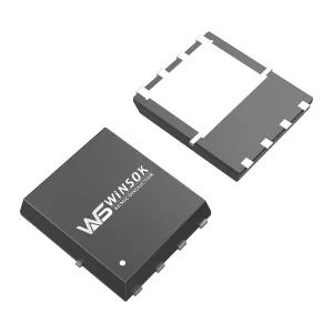
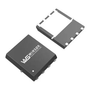
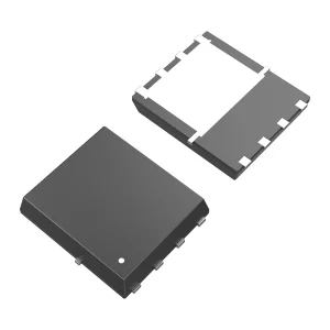
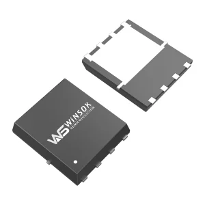
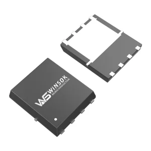
To achieve high current carrying capabilities up to 120A within small-footprint packages like the DFN5x6 (e.g., WSD20L120DN56), our factories utilize high-density trench gate structures. The scaling of cells allows a reduction in specific on-resistance ($R_{sp}$), allowing more silicon dies to fit into standard layouts without increasing package sizes.
For our medium-to-high voltage models (up to 650V), superjunction technology is employed. By establishing charge balance regions within the drift layers of the MOSFET, we decouple the historical physical trade-off between breakdown voltage ($V_{BR(DSS)}$) and on-state resistance. This technical shift reduces energy loss during fast switching transitions, yielding cooler running conditions.
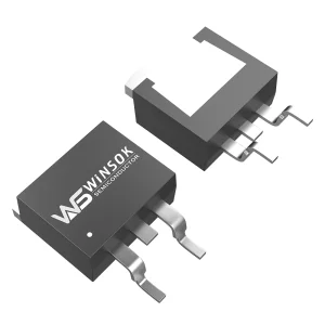
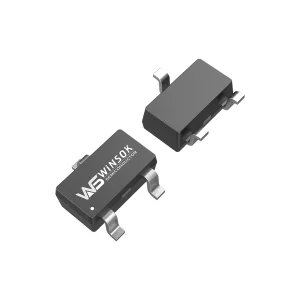
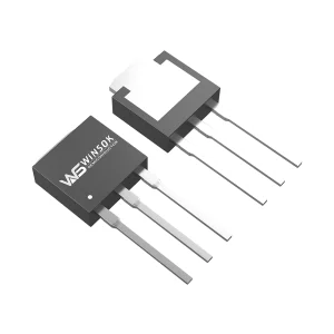
Leaded packages like the TO-220 or TO-262 introduce parasitic lead inductances that limit switching speed and generate electromagnetic interference (EMI). The automotive industry's push for power density has driven demand toward DFN5x6-8L and DFN3x3-8L packages.
Our roadmap focuses on expanding copper clip technology internally to eliminate wire bonds entirely. This optimization results in up to 50% lower package source inductance, significantly reducing switching voltage spikes and increasing thermal reliability under continuous-use EV conditions.
Aligning power discrete components with large-scale industrial and transportation ecosystems.
| Subsystem Application | Common Voltage Classes | Critical MOSFET Parametric Demands | Recommended Replacement Solution |
|---|---|---|---|
| BMS Protection & Balancing | 20V - 40V N-Ch / P-Ch | Extremely low $I_{GSS}$ leakage, thermal efficiency in compact packages | WSD20L120DN56 / WSD4078DN56 |
| On-Board Charger (OBC) | 60V - 150V Medium V | High surge current capacity, minimized $Q_g$, fast recovery body diodes | WSD80130DN56 / NTMFS6B14N equivalents |
| 12V/48V Auxiliary DC-DC | 30V - 100V Trench | Optimal switching figures of merit (FOM: $R_{DS(on)} \times Q_g$) | WSP4800 / WSD80130DN56 |
| EPS & HVAC Motor Drives | 40V - 80V Dual / Single N-Ch | Enhanced Safe Operating Area (SOA), high thermal cycling endurance | WSD4048DN56 / WSD4078DN56 |
As a global solution provider, Olukey Industry recognizes that components do not function in isolation. We offer complete system-level development support, bringing together WINSOK power discretes with Cmsemicon microcontrollers and customized PCBA engineering. This comprehensive, multi-layered approach ensures hardware compatibility, accelerates time-to-market, and minimizes integration risks for tier-1 automotive suppliers and industrial control manufacturers.
Global geopolitical changes and supply bottlenecks have highlighted the vital importance of building resilient supply chains. The modern Chinese fabrication plants and assembly lines partner with Olukey to provide reliable, high-yield manufacturing capacity.
By integrating automated visual inspection (AOI), real-time parametric testing, and automated wafer sorting systems, our manufacturing lines maintain stable, high-yield quality control. This operational scale enables stable component pricing and predictable lead times, even when traditional semiconductor channels face major disruptions.
With more than 600 models and over 40 distinct package configurations available, our supply chains are designed to handle both high-volume consumer orders and highly specialized industrial needs.





Quality and compliance are absolute priorities in international electronics procurement. Our components are designed, manufactured, and packaged to meet strict regulatory and quality benchmarks. Operating under ISO9001 and IATF 16949-aligned standards, every step of our manufacturing workflow is documented and traceable.
Additionally, all products comply with RoHS and REACH standards. This compliance ensures hassle-free import, export, and compliance validation when integrating these parts into assemblies destinated for highly regulated markets like Europe and North America.
To support localized design integration, we provide engineers with comprehensive design collateral, including S-parameter documentation, thermal models, SPICE simulations, and rapid physical evaluation samples.
Simplifying the transition from legacy western semiconductor brands to modern, cost-competitive alternatives.
Today's procurement strategies rarely rely on single-source components. Having pin-to-pin compatible, electrically equivalent secondary options is a proven method to prevent manufacturing halts.
WINSOK power components provide exact equivalents to many standard industry parts (such as the DFN5x6 series like NTMFS6B14N, SiR84DP, and TPH6R3ANL). These alternatives feature matched gate layouts, identical body footprints, and comparable thermal properties. This lets procurement and engineering departments swap parts with minimal to no layout adjustments.
HONGKONG Olukey INDUSTRY CO., LIMITED is an established solution provider focused on electronic product components. The company develops and delivers solutions across three main product lines: WINSOK MOSFETs, Cmsemicon MCUs, and custom PCBA circuit board solutions.
Today, Olukey Industry components are widely integrated into automotive electronics, aerospace and military applications, smart industrial control systems, new energy architectures, smart medical devices, 5G networking nodes, the Internet of Things (IoT), smart home infrastructure, and consumer electronics. Operating as a major general agent with direct factory relationships, we serve customers across the Asia-Pacific region and around the globe.
We combine deep technical expertise with hands-on logistics support to provide developers and manufacturers with advanced, high-reliability electronic components.
Guided by our foundational principles of "quality first, service first," we focus on building stable, long-term partnerships with high-tech enterprises and manufacturing plants worldwide.
WINSOK MOSFET focuses primarily on medium- and low-voltage technologies: 15V, 20V, 30V, 40V, 60V, 80V, 100V, 120V, 150V, 200V, 250V, 300V, 400V, 500V, 600V, and 650V options.
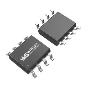
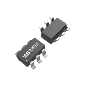
Our product lineup includes over 600 models housed in more than 40 package types (such as DFN3X3-8, DFN5X6-8, TO-252, TO-263, SOP-8, SOT-23, and TO-220). This provides broad component coverage for the global power electronics market.

Expert answers to common engineering, quality control, and component qualification questions.
To verify equivalency, we run a detailed comparison of three primary parameters: Electrical performance, thermal properties, and physical footprint. Electrically, we ensure that the breakdown voltage ($V_{(BR)DSS}$) meets or exceeds the original spec, and match both the gate charge ($Q_g$) and typical $R_{DS(on)}$ to keep efficiency within design tolerances. Thermally, we verify that the thermal resistance ($R_{\theta JC}$) can support the application's cooling setup. Physically, we confirm that pad layouts match exactly, avoiding PCB modifications during assembly.
Our high-current MOSFETs feature robust cell designs and thick copper clip internal bonding. This design choice bypasses the limitations of standard wire-bonds, which can melt under heavy surge currents. The solid copper structure minimizes internal package resistance ($R_{package}$), distributes thermal loads evenly across the die, and improves overall resistance to avalanche breakdown under inductive load switching.
During gate oxide formation, we maintain precise control over chemical vapor deposition (CVD) parameters. This ensures that the gate oxide layer thickness is uniform across the wafer. By keeping the gate threshold voltage within a narrow, predictable band, we prevent false turn-on events caused by fast voltage fluctuations ($dv/dt$) in noisy automotive or industrial environments.
Production takes place in ISO9001 and IATF 16949 certified facilities. These frameworks govern every step of the process, from raw wafer inspection to final dicing, packaging, and testing. Additionally, components comply with REACH and RoHS standards, ensuring they meet the environmental requirements of global markets.
High-reliability components designed for motor drives, load switches, and battery protection networks.

 Olukey