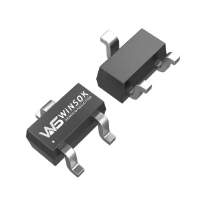
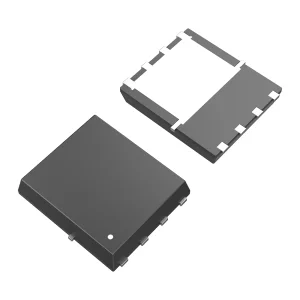
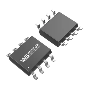
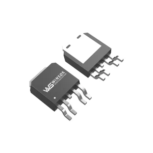
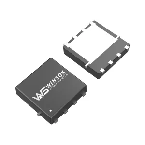
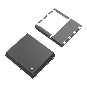
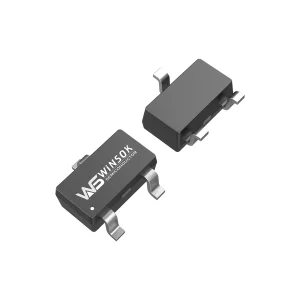
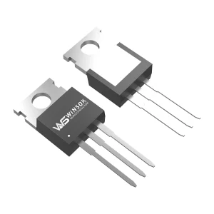
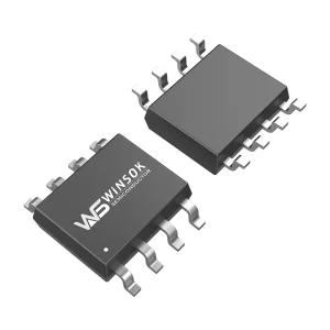
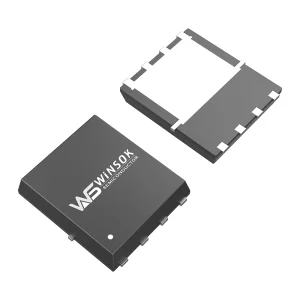
Explore our production-ready, industry-standard MOSFET topologies engineered for maximum power density and efficient heat dissipation.
Understanding the technical demands and market trajectory of battery management systems in an electrified economy.
The global transition toward electrification, driven by Electric Vehicles (EVs), grid-scale Energy Storage Systems (ESS), telecom backup power, and portable smart electronics, has elevated the critical status of the Battery Management System (BMS). Within a BMS, the power MOSFET acts as a critical safety valve and dynamic switch, managing charging, discharging, and safety cutoff functions.
Engineers worldwide face the challenge of sourcing power semiconductors that can handle large currents while minimizing heat generation. Modern BMS architectures demand MOSFETs with exceptionally low Static Drain-Source On-Resistance (Rds(on)) and optimized Gate Charge (Qg) characteristics. This prevents thermal runaway and ensures maximum energy efficiency.
From micro-mobility solutions like e-bikes requiring 30V-60V MOSFETs, to large-scale utility batteries operating at high voltages, the requirement for robust, reliable, and cost-effective power semiconductors is surging exponentially. Manufacturers are actively shifting from standard discrete components to customized, application-specific ODM solutions to build highly integrated, fault-tolerant BMS modules.
Why leading global electronics brands rely on South China semiconductor clusters for customized power MOSFET supplies.

China's Greater Bay Area (Shenzhen, Hong Kong, and Dongguan) represents the world’s most integrated hardware ecosystem. For global procurement teams looking to buy power MOSFETs for BMS, the local supply chain offers structural advantages that cannot be replicated elsewhere:
Your integrated electronic components solution provider bridging global demand with reliable semiconductor engineering.
HONGKONG Olukey INDUSTRY CO., LIMITED is an established solution provider focusing on the overall engineering and delivery of premium electronic component systems. Our product portfolio spans three core lines: WINSOK MOSFETs, Cmsemicon MCUs, and specialized PCBA circuit board development.
Presently, Olukey Industry's components are deployed across automotive electronics, aerospace/military applications, smart industrial control systems, new energy projects, smart medical diagnostic equipment, 5G base stations, IoT node devices, and consumer products. Relying on deep relationships with original semiconductor manufacturers and global agents, we offer end-to-end component sourcing, technical support, and logistical security in the Asia-Pacific region and beyond.
Our strategic alignment with leading fabrication plants and packaging facilities allows us to guarantee consistent lead times. By integrating digital solutions like microcontrollers (MCUs) alongside Winsok's comprehensive range of power devices, we help electronic manufacturers develop highly optimized, drop-in replacement solutions that lower bill-of-materials (BOM) costs while mitigating supply chain disruption risks.




Combining high-performance silicon structures with specialized thermal packages to drive efficiency in BMS design.


A technical blueprint illustrating typical application scenarios and recommended design topologies for specific battery configurations.
| BMS Voltages (Cell Count) | Recommended MOSFET VDS | Optimal Packaging Type | Key Performance Metrics |
|---|---|---|---|
| 3.7V - 12V (1S - 3S) | 20V - 30V | DFN3X3-8, SOP-8, SOT-23 | Ultra-low Rds(on) < 2mΩ, small footprint, low gate charge. |
| 12V - 24V (4S - 7S) | 40V - 60V | DFN5X6-8, SOP-8 | Balanced switching loss, excellent RDS(on) thermal stability. |
| 36V - 48V (10S - 13S) | 80V - 100V | DFN5X6-8, TO-252, TO-220 | High avalanche energy capability, low transient thermal impedance. |
| 60V - 96V+ (16S - 24S+) | 120V - 150V+ | TO-263, TO-220, Custom DFN | Superior dV/dt ruggedness, high current handling capacity. |
Essential design-in and purchasing guidelines for global procurement managers and hardware design engineers.
When selecting an ODM Power MOSFET for BMS, engineering and procurement teams must align on several critical milestones to secure product longevity, system safety, and overall reliability:
While low Rds(on) is critical to minimize steady-state conduction loss, designers must also evaluate Safe Operating Area (SOA) curves and transient thermal impedance. During short-circuit conditions, the MOSFET must survive high currents for microseconds before the MCU or analog front-end (AFE) triggers a shutdown.
In high-current switching applications, lead frame packages like the TO-220 introduce higher parasitic source inductance, which can trigger ringing at the gate. Modern designs favor leadless packages like DFN5X6-8, which feature low internal package resistance and direct copper clip bonding for reduced parasitic noise.
To avoid single-point failure risks in supply chains, modern OEM policies require secondary sourcing. Winsok's product family is engineered to match industry-standard footprints (e.g., standard SOP-8, DFN, TO footprints), facilitating smooth drop-in replacements during engineering validation tests (EVT) or mass production.
Technical answers addressing the most common issues raised by circuit designers and electronics buyers.
In battery management systems, MOSFETs usually operate in the fully on-state to allow continuous charging or discharging currents. The power loss ($P = I^2 \times R_{DS(on)}$) directly correlates to thermal dissipation. Reducing Rds(on) minimizes temperature rise within the packed battery enclosure, increasing safety and battery life.
Custom ODM solutions let engineers adjust specific parameters like breakdown voltage margins, packaging profiles (e.g., dual-channel vs. single), package thickness for slim consumer electronics, and optimized gate charges. This allows the power stage to match the driver capabilities of specialized BMS AFEs.
We recommend a safety margin of at least 1.5 to 2 times the maximum charging voltage of the battery pack. This buffers the system against inductive voltage spikes during sudden load shut-offs or short circuits. For instance, a 48V battery pack generally uses 80V or 100V MOSFETs.
DFN5X6-8 and TO-252 packages are highly recommended. DFN packages minimize thermal resistance from junction to case ($R_{thJC}$) while occupying minimal PCB area. For extreme current demands, multiple DFN5X6-8 or TO-263 packages can be placed in parallel.
Always implement transient voltage suppressors (TVS diodes) close to the gate-source terminals to clamp spikes. Ensuring the gate driver voltage stays well below the MOSFET’s maximum $V_{GS}$ limit (typically ±20V) also prevents gate oxide failure.
Select from our production-tested, low-resistance MOSFET lines designed for high-current applications.

 Olukey