Deploy next-generation switching architectures with these highly reliable, low RDS(on) P-Channel MOSFETs tuned for the demanding environmental and power profiles of Boston industrial applications.
Boston and the broader New England region represent one of the world's most dense concentrations of high-technology research labs, autonomous systems startups, biomedical electronics giants, and defense innovators. Driven by academic powerhouse centers like MIT, Harvard, and Northeastern University, the local market demands semiconductor components that do not merely meet baseline data sheet specs, but exceed thermal limits under severe real-world operational constraints.
P-Channel MOSFETs play a crucial, non-substitutable role in high-side load switching, reverse polarity protection circuits, and smart battery management units (BMUs). By eliminating the need for an external charge pump or complex bootstrap drive circuit required by N-channel counterparts, P-channel components simplify driver design, minimize EMI signatures, and dramatically save board real estate. In robotics actuation, laboratory centrifuge controls, and subsea oceanographic imaging systems, this reliability represents the boundary between system success and catastrophic downtime.

Understanding the physics of hole-mobility, packaging advancements, and thermal mechanics is paramount when sourcing P-Channel MOSFETs for harsh industrial and biotech systems.
N-channel MOSFETs need a gate voltage higher than the supply rail (typically via a bootstrap circuit) to turn on when placed high-side. A P-channel MOSFET turns on with a simple gate voltage below the source rail. This fundamentally reduces passive component counts in space-constrained IoT and drone boards.
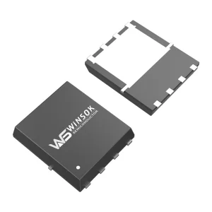
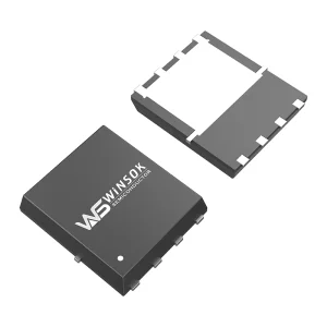
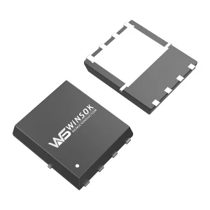
Silicon hole mobility is naturally 2-3 times lower than electron mobility. Consequently, for equivalent die sizes, P-channel devices exhibit higher RDS(on). Selecting ultra-trench designs like our DFN3x3 and DFN5x6 series offsets this physical limitation, ensuring sub-10mΩ resistance targets are met.
Battery-powered systems face user-error risks. Using a P-channel MOSFET in place of a series diode for reverse polarity protection drastically reduces power dissipation (I2R vs. VF*I), conserving operational battery life and managing thermal spikes inside hermetic equipment.
These components offer high packaging densities and excellent thermal management performance, critical for marine instrumentation and automated battery swap systems in Greater Boston.

HONGKONG Olukey INDUSTRY CO., LIMITED is a solution provider focusing on the overall solution of electronic product components. The main products mainly include: WINSOK MOSFET, Cmsemicon MCU, PCBA circuit board solution development and other three types of product lines.
At present, the products of Olukey Industry are widely used in automotive electronics, military electronics, smart industry, new energy, smart medical care, 5G, Internet of Things, smart home, and various consumer electronics products. Relying on the advantages of global general agents of major original factories, we are based in the Asia-Pacific market. Provide customers with various advanced high-tech electronic components by using comprehensive superior services, assist manufacturers in producing high-quality products and provide comprehensive services.
Mitigating semiconductor lead times through drop-in replacements and structural engineering alternatives.
The global semiconductor market has shown how vulnerable single-source designs are to geopolitical shifts, factory fires, and logistics logjams. Procurement teams in the Boston market increasingly enforce dual-source policies.
Olukey Industry provides cross-reference configurations targeting major industry brands. We replace configurations from Alpha & Omega Semiconductor (AOS), NIKO Semi, and Potens Semiconductor with equivalent form, fit, and function components. Our products match the pinouts, footprint dimensions, and electrical parameters (gate threshold voltage VGS(th), total gate charge Qg, thermal resistance RθJC) of historical market parts, minimizing layout re-design costs.
Cross-reference matrix matching makes switching components stress-free during production scale-up phases.
| Industry Part (AOS/NIKO/Potens) | Winsok Drop-in Replacement | Thermal Package |
|---|---|---|
| AON6411 | WSD30L120DN56 | DFN5x6-8 |
| PK5A7BA | WSD30L68DN33 | DFN3x3-8L |
| PDC3901X | WSD40L48DN33 | DFN3x3-8L |
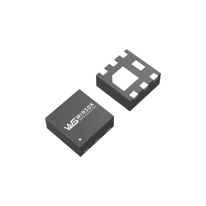
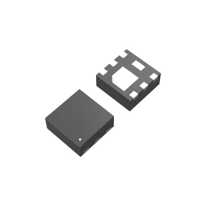
| AON2409 | WSD1216DN22 | DFN2x2-6L |
We use comprehensive high-quality services to provide customers with various types of advanced high-tech electronic components, assist manufacturers in producing high-quality products and provide comprehensive services. Over the years, the company has relied on reputation to survive, adhering to the tenet of "quality first, service first", and has established good cooperative relationships with many high-tech enterprises and original manufacturers at home and abroad.
Relying on the advantages of global general agents of major original manufacturers, we are based on the Asia-Pacific market. Through active market development and effective resource integration, it has become one of the outstanding and fast-growing agents in the Asia-Pacific region. The company has many years of professional distribution experience. We use our comprehensive advantageous services to provide customers with various types of advanced high-tech electronic components, assist manufacturers in producing high-quality products and provide comprehensive services.




WINSOK MOSFET's product voltages are mainly medium and low voltage: 15V, 20V, 30V, 40V, 60V, 80V, 100V, 120V, 150V, 200V, 250V, 300V, 400V, 500V, 600V, 650V. The main packages include DFN3X3-8, DFN5X6-8, TO-252, TO-263, SOP-8, SOT-23, TO-220, etc. There are more than 600 models and more than 40 packages. Extensive coverage of medium-voltage and low-voltage MOSFET product lines on the market.
Cmsemicon MCU is a microcontroller company born in Shenzhen, with rich product types and technology research and development experience.
Becoming a global high-value agent is the common goal pursued by OLUKEY Industrial employees. We adhere to the corporate values of "Pragmatism, Win-win, Service and Responsibility", continue to strengthen service quality, and aim to provide high-quality services. Work hand in hand with suppliers to jointly explore a larger market and contribute to the prosperity and development of semiconductors.

High-density modern systems require advanced thermal dissipation models to handle peak switching stresses.
Traditional packages like SOP-8 or TO-220 rely on long wire bonds internally to connect the silicon die to the external leads. These wires induce parasitic inductance, which leads to voltage ringing and switching losses at high frequencies.
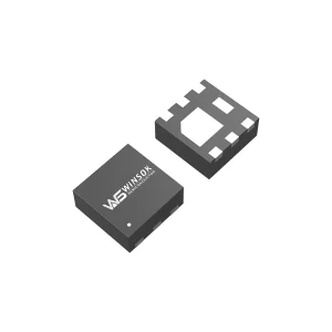
Dual Flat No-Lead (DFN) packaging, such as the DFN2x2, DFN3x3, and DFN5x6, utilizes direct copper clip bonding. This design lowers package electrical resistance and minimizes thermal impedance. As robotic actuary drives in Boston labs increase operating frequencies to shrink inductor sizes, selecting clip-bonded DFN P-Channel MOSFETs becomes a non-negotiable step in maintaining design stability.
Explore our primary inventory of high-reliability P-Channel MOSFETs, featuring drop-in compatibility and direct factory warranties.

Boston's defense and aerospace technology hubs require components manufactured under strict process control. To support these standards, Olukey Industry operates under a quality assurance framework where every wafer run undergoes extensive parametric inspection.
Our P-channel MOSFET series are fully compliant with RoHS and REACH regulations, eliminating environmental risk flags in your bill of materials (BOM). We provide complete component traceability, detailed failure analysis support, and AEC-Q101 qualified options for high-reliability automotive and medical equipment.
For custom engineering requirements, our applications group works directly with development teams to select target products, design safe thermal limits, and model circuit simulations.
Get fast answers to critical engineering and logistical questions regarding P-Channel MOSFET applications.
Don't let semiconductor component shortages slow your product development. Partner with a reliable distributor to secure factory-backed parts, request customized packaging, and download detailed cross-reference lists.
 Olukey